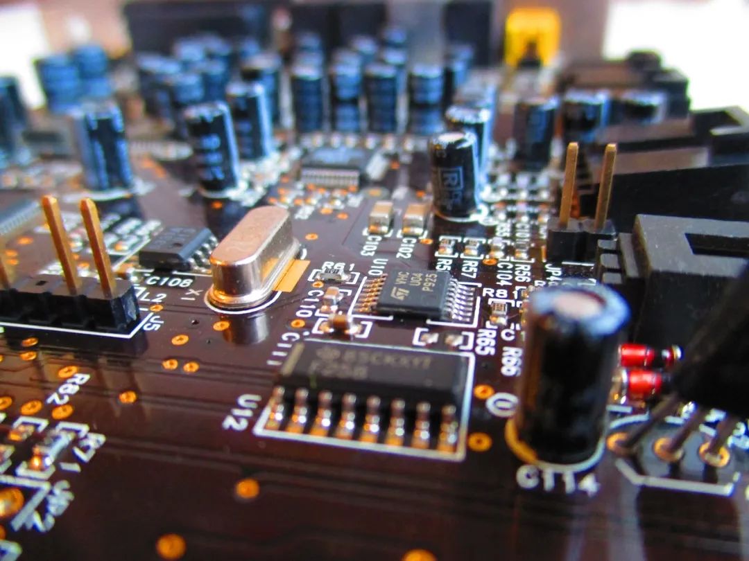
In PCB design, we often encounter the two technical terms “Via” and “Pad.” They each have distinct functions and uses. This article will detail the differences and roles of these two elements, hoping to assist everyone.

1. Via, also known as a via, is primarily used to achieve electrical connections between different layers. Depending on structural characteristics, vias can be categorized into three types: through-hole, blind hole, and buried hole. Through-holes run through the entire PCB, while blind holes terminate at a specific layer of the PCB, and buried holes are completely embedded within the PCB. During PCB production, the diameter of vias is usually not strictly controlled, as their main function is electrical connection rather than mechanical fixation. To improve production efficiency, similar vias may sometimes be combined for production to reduce tool change times. Additionally, due to spacing and width limitations, the diameter of vias may also be appropriately adjusted. It is worth noting that the surface of vias can be coated with solder mask ink or left uncoated, depending on specific design requirements.
2. Pad, which refers to a pad, is primarily used for soldering component leads to achieve electrical connections and mechanical fixation. Pads are divided into two types: pin pads and surface mount pads. Pin pads typically have solder holes for soldering pin components, while surface mount pads do not have solder holes and are suitable for soldering surface mount components. During PCB production, the diameter of pads must be strictly controlled, with tolerances generally maintained within ±0.08mm. This is because the diameter of the pad must be large enough to ensure that component leads can pass through smoothly. If the diameter is too small, it will result in improper installation of the components, or even damage to the pad. Furthermore, the surface of the pad must remain clean and free of contaminants such as solder mask ink. This is because solder mask ink can affect soldering quality, leading to poor soldering or component detachment.
This article is an original piece by Fanyi Enterprise Training. Please cite the source if reproduced!
Submissions/Recruitment/Advertisement/Course Collaboration/Resource Exchange; please add WeChat: 13237418207