

To avoid rewriting the SPI driver every time, we parameterize it to make it as efficient as possible.What is the use of SPI master? You will find that the configuration of various peripheral chips is generally done through SPI, whether it’s three-wire or four-wire.What is the use of SPI slave? When the external host (CPU) needs to read the internal register values of the FPGA, it becomes very useful. The FPGA registers are akin to RAM, allowing the CPU to read and write data via SPI.The code is for reference only and should not be used for commercial purposes.

SPI Slave
Features supported by SPI slave:
-
Support for three-wire or four-wire SPI, switchable via define. -
Support for custom instruction length and frame length. -
Customizable working clock, greater than twice the SPI clock.
The user only needs to modify: (1) the number of wires in SPI. (2) single frame length. (3) instruction length. (4) register allocation.
Note: The highest bit of the instruction indicates read/write, low indicates write and high indicates read, while the remaining bits indicate the address. The instruction is followed by the data port, and the sum of their widths is the length of a single SPI frame.
//`define SPI_LINE  //Is it three-wire SPI`define SPI_FRAME_WIDTH 16 //SPI frame length is 16`define SPI_INS_WIDTH 8    //SPI instruction length`timescale 1ns/1ps////module spi_slave (    input     i_clk               , //work clk    input     i_rst_n             ,        input     i_spi_clk           , //SPI clk    input     i_spi_cs            , //SPI cs
    `ifdef SPI_LINE                 // Conditional compilation    inout     io_spi_sdio              `else    input     i_spi_mosi          , //SPI mosi    output    o_spi_miso            //SPI miso    `endif          );// Bit width calculation functionfunction integer clogb2 (input integer depth);begin    for (clogb2=0; depth>0; clogb2=clogb2+1)         depth = depth >>1;                          endendfunctionreg r_cs = 1'b1; // One beat always @(posedge i_clk)begin    r_cs <= i_spi_cs;endreg [1:0] r_spi_clk_edge = 2'b00; // SPI clock edge detectionalways @(posedge i_clk)begin    r_spi_clk_edge <= {r_spi_clk_edge[0],i_spi_clk};end //alwaysreg [clogb2(`SPI_FRAME_WIDTH-1)-1:0] r_spi_cnt = 'd0;always @(posedge i_clk)begin    if (r_cs) // cs is high, reset to zero        r_spi_cnt <= 'd0;    else if (r_spi_clk_edge == 2'b10) // Count only on falling edge        r_spi_cnt <= r_spi_cnt + 'd1;end//// Instruction latchreg [`SPI_INS_WIDTH-1:0] r_ins = 'd0;always @(posedge i_clk)begin    if ((~r_cs) && (r_spi_clk_edge == 2'b01)) // Latch data on rising edge    begin        if ((r_spi_cnt >= 0) && (r_spi_cnt <= `SPI_INS_WIDTH-1))        `ifdef SPI_LINE                 // Conditional compilation            r_ins <= {r_ins[`SPI_INS_WIDTH-2:0],io_spi_sdio};          `else            r_ins <= {r_ins[`SPI_INS_WIDTH-2:0],i_spi_mosi};          `endif     end end//// Data writingreg [`SPI_FRAME_WIDTH-`SPI_INS_WIDTH-1:0] r_data_rx = 'd0;always @(posedge i_clk)begin    if ((~r_cs) && (r_spi_clk_edge == 2'b01)) // Latch data on rising edge    begin        if (r_spi_cnt >= `SPI_INS_WIDTH)        `ifdef SPI_LINE            r_data_rx <= {r_data_rx[`SPI_FRAME_WIDTH-`SPI_INS_WIDTH-2:0],io_spi_sdio};        `else            r_data_rx <= {r_data_rx[`SPI_FRAME_WIDTH-`SPI_INS_WIDTH-2:0],i_spi_mosi};           `endif    endend//// User register definitionsreg [`SPI_FRAME_WIDTH-`SPI_INS_WIDTH-1:0] r_reg0 = 'd0;reg [`SPI_FRAME_WIDTH-`SPI_INS_WIDTH-1:0] r_reg1 = 'd0;reg [`SPI_FRAME_WIDTH-`SPI_INS_WIDTH-1:0] r_reg2 = 'd0;reg [`SPI_FRAME_WIDTH-`SPI_INS_WIDTH-1:0] r_reg3 = 'd0;////always @(posedge i_clk,negedge i_rst_n)begin    if (~i_rst_n)    begin        r_reg0 <= 'd0;        r_reg1 <= 'd0;        r_reg2 <= 'd0;        r_reg3 <= 'd0;
    end    else if ((~r_ins[`SPI_INS_WIDTH-1]) && (r_spi_cnt == (`SPI_FRAME_WIDTH-1)) && (~r_cs) && (r_spi_clk_edge == 2'b01))    begin    `ifdef SPI_LINE        case (r_ins[`SPI_INS_WIDTH-2:0])            'd0:begin r_reg0 <= {r_data_rx[`SPI_FRAME_WIDTH-`SPI_INS_WIDTH-2:0],io_spi_sdio}; end            'd1:begin r_reg1 <= {r_data_rx[`SPI_FRAME_WIDTH-`SPI_INS_WIDTH-2:0],io_spi_sdio}; end            'd2:begin r_reg2 <= {r_data_rx[`SPI_FRAME_WIDTH-`SPI_INS_WIDTH-2:0],io_spi_sdio}; end            'd3:begin r_reg3 <= {r_data_rx[`SPI_FRAME_WIDTH-`SPI_INS_WIDTH-2:0],io_spi_sdio}; end
        endcase     `else        case (r_ins[`SPI_INS_WIDTH-2:0])            'd0:begin r_reg0 <= {r_data_rx[`SPI_FRAME_WIDTH-`SPI_INS_WIDTH-2:0],i_spi_mosi}; end            'd1:begin r_reg1 <= {r_data_rx[`SPI_FRAME_WIDTH-`SPI_INS_WIDTH-2:0],i_spi_mosi}; end            'd2:begin r_reg2 <= {r_data_rx[`SPI_FRAME_WIDTH-`SPI_INS_WIDTH-2:0],i_spi_mosi}; end            'd3:begin r_reg3 <= {r_data_rx[`SPI_FRAME_WIDTH-`SPI_INS_WIDTH-2:0],i_spi_mosi}; end
        endcase     `endif     end
end//// Register value readoutreg [`SPI_FRAME_WIDTH-`SPI_INS_WIDTH-1:0] r_data_tx = 'd0;always @(posedge i_clk)begin    if (r_ins[`SPI_INS_WIDTH-1] && (~r_cs) && (r_spi_clk_edge == 2'b10))    begin         if (r_spi_cnt == (`SPI_INS_WIDTH-1))        begin            case (r_ins[`SPI_INS_WIDTH-2:0])                'd0:begin r_data_tx <= r_reg0; end                 'd1:begin r_data_tx <= r_reg1; end                 'd2:begin r_data_tx <= r_reg2; end                 'd3:begin r_data_tx <= r_reg3; end                 endcase         end        else             r_data_tx <= {r_data_tx[`SPI_FRAME_WIDTH-`SPI_INS_WIDTH-2:0],1'b0};    end end
//// Read output`ifdef SPI_LINEassign io_spi_sdio = (r_ins[`SPI_INS_WIDTH-1]) ? (((r_spi_cnt>=`SPI_INS_WIDTH) && (r_spi_cnt<`SPI_FRAME_WIDTH)) ? r_data_tx[`SPI_FRAME_WIDTH-`SPI_INS_WIDTH-1] : 1'bz) : 1'bz;`else assign o_spi_miso = ((r_spi_cnt>=`SPI_INS_WIDTH) && (r_spi_cnt<`SPI_FRAME_WIDTH)) ? r_data_tx[`SPI_FRAME_WIDTH-`SPI_INS_WIDTH-1] : 1'b0;`endif
endmodule // end the spi_slave model
SPI Master
The SPI master only encapsulates the SPI driver, while the control of writing values and reading them is handled by the upper layer, which is simple and will not be elaborated. Users only need to provide the SPI frame and control enable.
The user only needs to modify parameter parameters: (1) single frame length; (2) instruction length; (3) data length; (4) working clock; (5) SPI clock.
The implementation does not use a state machine but adopts a linear sequence counting method.
//`define SPI_LINE  //Is it three-wire SPI`timescale 1ns/1psmodule spi_master #(parameter p_spi_frame_width = 16, //SPI single frame length  parameter p_spi_ins_width = 8   , //Instruction length  parameter p_spi_data_width = 8    //Data length for reading)(    input                                i_clk             , //System clock    input                                i_rst_n           ,    input                                i_flag            , // Detect rising edge of flag to start a transmission, one clock cycle is sufficient       input     [p_spi_frame_width-1:0]    i_spi_data        ,    output                               o_spi_cs          ,    output                               o_spi_clk         ,
    `ifdef SPI_LINE                 // Conditional compilation    inout                                io_spi_sdio       ,              `else    input                                i_spi_miso        , //SPI miso    output                               o_spi_mosi        , //SPI mosi    `endif         output                               o_transfer_done   , // Single transmission complete    output    [p_spi_data_width-1:0]     o_spi_data          // Read data           );parameter p_clk_fre = 200; //XXM clock frequencyparameter p_spi_clk_fre = 0.5*1000; //SPI clock rate, indicating 1Mparameter p_clk_div = p_clk_fre * 1000/p_spi_clk_fre/2-1;parameter p_spi_cnt_max = p_spi_frame_width*2-1;parameter p_spi_ins_max = p_spi_ins_width*2-1;// Bit width calculation functionfunction integer clogb2 (input integer depth);begin    for (clogb2=0; depth>0; clogb2=clogb2+1)         depth = depth >>1;                          endendfunction// Assign the maximum value to the linear, directly using p_clk_div for simulation has issues, but it works on the boardwire [clogb2(p_clk_div)-1:0] w_clk_div;assign w_clk_div = p_clk_div;//// Clock divisionreg [clogb2(p_clk_div)-1:0] r_cnt_div = 'd0;always @(posedge i_clk)begin    if (r_cnt_div == w_clk_div)        r_cnt_div <= 'd0;    else         r_cnt_div <= r_cnt_div + 'd1;end //alwayswire w_clk_en; // Division clock enableassign w_clk_en = (r_cnt_div == w_clk_div) ? 1'b1 : 1'b0;reg [1:0] r_flag_edge = 2'b00;reg [clogb2(p_spi_cnt_max)-1:0] r_spi_cnt = 'd0;always @(posedge i_clk) // Detect flag edgebegin    r_flag_edge <= {r_flag_edge[0],i_flag};end// Flag signal wide to low-speed clock domainreg r_flag_enlarge = 1'b0;always @(posedge i_clk)begin    if (r_flag_edge == 2'b01) // Raise on rising edge        r_flag_enlarge <= 1'b1;    else if (r_spi_cnt == p_spi_ins_max) // Only pull low when the high level is long enough        r_flag_enlarge <= 1'b0;endreg [1:0] r_flag_enlarge_edge = 2'b00;always @(posedge i_clk)begin    if (w_clk_en)        r_flag_enlarge_edge <= {r_flag_enlarge_edge[0],r_flag_enlarge};endreg r_cs = 1'b1;always @(posedge i_clk)begin    if (w_clk_en)    begin        if (r_flag_enlarge_edge == 2'b01) // Detected need for SPI operation            r_cs <= 1'b0;        else if (r_spi_cnt == p_spi_cnt_max) // Counting to the maximum value indicates one SPI completion            r_cs <= 1'b1;    endendalways @(posedge i_clk)begin    if (w_clk_en)    begin        if(~r_cs) // Count in the operational area            r_spi_cnt <= r_spi_cnt + 'd1;        else             r_spi_cnt <= 'd0;    end    end//// Data transfer segmentreg [p_spi_frame_width-1:0] r_data = 'd0;always @(posedge i_clk)begin    if (w_clk_en)    begin        if (r_flag_enlarge_edge == 2'b01) // Raise on rising edge            r_data <= i_spi_data;        else if (r_spi_cnt[0] == 1'b1) // Data moves            r_data <= {r_data[p_spi_frame_width-2:0],1'b1};    endend//// Data reading segmentreg [p_spi_data_width-1:0] r_data_read = 'd0;always @(posedge i_clk)begin    if (w_clk_en)    begin        if (i_spi_data[p_spi_frame_width-1] && (r_spi_cnt > p_spi_ins_max) && (r_spi_cnt[0] == 1'b0)) // Read        `ifdef SPI_LINE            r_data_read <= {r_data_read[p_spi_data_width-2:0],io_spi_sdio};        `else            r_data_read <= {r_data_read[p_spi_data_width-2:0],i_spi_miso};        `endif     end    end//// SPI output segmentassign o_spi_cs = r_cs;assign o_spi_clk = r_cs ? 1'b0 : r_spi_cnt[0];//// SPI SDIO input/output switching`ifdef SPI_LINEassign io_spi_sdio = (i_spi_data[p_spi_frame_width-1]) ? (((r_spi_cnt >= 'd0) && (r_spi_cnt <= p_spi_ins_max)) ? r_data[p_spi_frame_width-1] : 1'bz ) : r_data[p_spi_frame_width-1];`else assign o_spi_mosi = r_data[p_spi_frame_width-1];`endif assign o_transfer_done = ((~r_cs) && (r_spi_cnt == p_spi_cnt_max)) ? 1'b1:1'b0;assign o_spi_data = r_data_read;
endmodule // end the spi_master model
Simulation is shown below: Write values to four registers and then read them.
The simulation code is as follows:
`define TRANSFER_NUMBER 8 // Number of operations is 4`define DATA 8'ha5//`define SPI_LINEtimeunit 1ns;timeprecision 1ps;module top;parameter p_sim_end_time = 1000000; //nslogic l_clk = 1'b0;always #2.5 l_clk = ~l_clk;//// Reset logic l_rst_n  = 1'b0;initial begin    #100 l_rst_n = 1'b1;end
wire io_sdio;wire o_spi_cs;wire o_spi_clk;wire o_transfer_done;wire [7:0] o_spi_data;//// Multiple data operation modesreg r_flag = 1'b0;reg [1:0] r_first_cnt = 2'b00;always @(posedge l_clk,negedge l_rst_n)begin    if (~l_rst_n)        r_first_cnt <= 2'b00;    else if (r_first_cnt == 2'd3)        r_first_cnt <= r_first_cnt;    else         r_first_cnt <= r_first_cnt + 2'd1;endreg [1:0] r_transfer_done_edge = 2'b00;always @(posedge l_clk)begin    r_transfer_done_edge <<= {r_transfer_done_edge[0],o_transfer_done};endreg [3:0] r_transfer_cnt = 4'd0;always @(posedge l_clk)begin    if ((r_first_cnt == 2'd2) && (r_transfer_cnt < `TRANSFER_NUMBER))        r_flag <= 1'b1;    else if ((r_transfer_done_edge == 2'b10) && (r_transfer_cnt < `TRANSFER_NUMBER-1))        r_flag <= 1'b1;    else         r_flag <= 1'b0;        endalways @(posedge l_clk)begin    if (r_transfer_done_edge == 2'b10)        r_transfer_cnt <= r_transfer_cnt + 'd1;endreg [15:0] r_in_data  = 16'd0;always @(*)begin    if (~l_rst_n) // Simulation does not execute this segment, there will be issues        r_in_data  = 16'h0000;    else     begin     case(r_transfer_cnt)        4'd0:begin  r_in_data  = {8'h00,8'h43}; end         4'd1:begin  r_in_data  = 16'h0132; end         4'd2:begin  r_in_data  = 16'h0245; end         4'd3:begin  r_in_data  = 16'h0367; end         4'd4:begin  r_in_data  = 16'h8000; end         4'd5:begin  r_in_data  = 16'h8100; end         4'd6:begin  r_in_data  = 16'h8200; end         4'd7:begin  r_in_data  = 16'h8300; end
        default:begin  r_in_data  = 16'h0000; end    endcase    end end
wire w_spi_miso;wire w_spi_mosi;
spi_master inst_spi_master (    .i_clk             (l_clk),    .i_rst_n           (),    .i_flag            (r_flag),    .i_spi_data        (r_in_data),    .o_spi_cs          (o_spi_cs),    .o_spi_clk         (o_spi_clk),    `ifdef SPI_LINE    .io_spi_sdio       (io_sdio),    `else    .i_spi_miso        (w_spi_miso),    .o_spi_mosi        (w_spi_mosi),    `endif    .o_transfer_done   (o_transfer_done),    .o_spi_data        (o_spi_data)    );
spi_slave  inst_spi_slave (    .i_clk                            (l_clk),    .i_rst_n                          (l_rst_n),
    .i_spi_clk                        (o_spi_clk),    .i_spi_cs                         (o_spi_cs),    `ifdef SPI_LINE    .io_spi_sdio                      (io_sdio)    `else    .i_spi_mosi                      (w_spi_mosi),    .o_spi_miso                      (w_spi_miso)    `endif
);
initial begin    #p_sim_end_time $stop;end
    endmodule
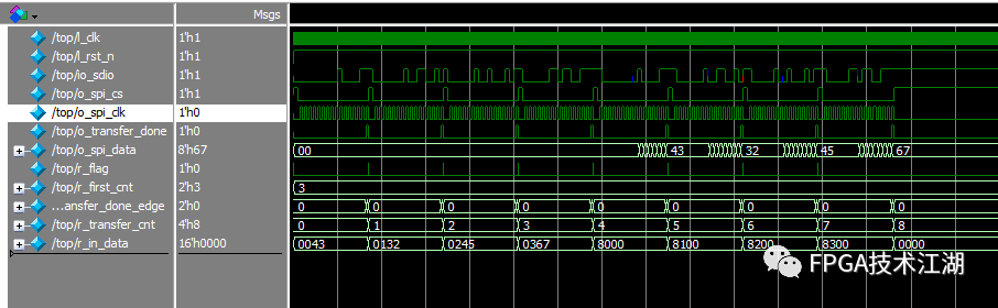
Four-Wire SPI: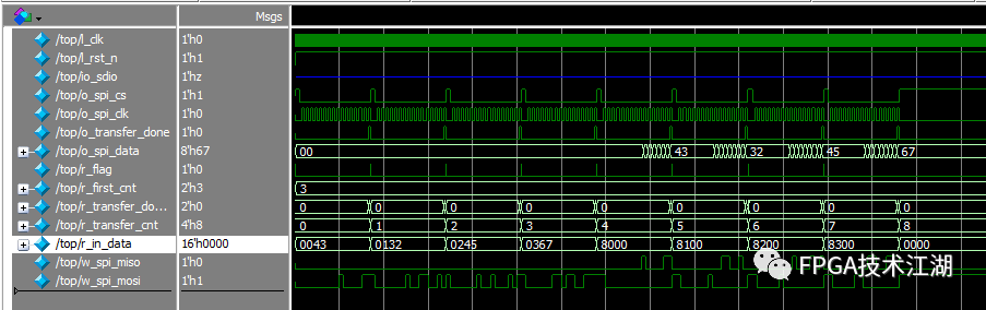
You can see that the read and write operations are consistent, and the verification is successful.
– THE END –
🍁
Selected Past Articles


[Free] FPGA Engineer Recruitment Platform
FPGA talent recruitment, HR of enterprises, pay attention!
Selected System Design | Real-time Image Edge Detection System Design Based on FPGA (with code)
Gigabit Ethernet RGMII Interface Design Based on Primitives
Timing Analysis Theory and TimeQuest Usage_ Chinese Edition
Job Interview | Latest Compilation of FPGA or IC Interview Questions
Data Compilation | FPGA Software Installation Packages, Books, Source Code, Technical Documents… (Updated on 2024.01.06)
FPGA Employment Class, starting on 05.04, new course content at no extra charge, high salary employment, online and offline synchronization!


FPGA Technology Community Broadly Issues Community Posts
No advertisements in pure mode, providing a pure land for technical exchanges, from beginners to industry elites and big shots, from military to civilian enterprises, covering various directions from communication, image processing to artificial intelligence, QQ WeChat double selection, FPGA technology community builds the purest and most professional technical exchange learning platform.
FPGA Technology Community WeChat Group

Add the group owner’s WeChat, note your name + school/company + major/position to join the group
FPGA Technology Community QQ Group

Note: Name + School/Company + Major/Position to join the group