 Low Power Design Methods – Considerations for Frequency and Voltage Scaling
-
Level Shifters and Isolation
In any multi-voltage design, level shifters are required at the interfaces of modules operating at different voltages. If the DVFS block is power-gated, we also need to isolate the output.
Note that implementing a level shifter that only moves in one direction is much easier. This means that the voltage of the DVFS block must always be higher than the voltage of the block it is connected to, or it must always operate at a lower voltage.
Due to the lack of voltage headroom in RAM, in most DVFS CPU designs, the cache is always at a voltage higher than or equal to that of the CPU.
While theoretically the bus interface voltage of the CPU can be higher or lower, for practical reasons, the bus is usually kept at a voltage higher than or equal to that of the CPU. The characteristics of the bus interface unit are typically not as carefully managed, and running it at or below the CPU’s minimum voltage may lead to system errors.
-
Voltage Scaling Interfaces – Impact on Synchronous Timing
As the DVFS block changes voltage and frequency, the timing of the synchronous interfaces between the DVFS block and the rest of the system becomes more complex.
With voltage changes in the DVFS module, the clock tree delays also change. It is not possible to assign a single low-skew clock to both the DVFS module and the system to maintain low skew across all voltages. Therefore, the standard model for synchronous interfaces breaks down.
One solution is to use asynchronous interfaces. A configuration of the ARM1176 that enables DVFS adopts this approach. It provides an asynchronous interface for the AXI bus, equipped with bidirectional synchronizers. These synchronizers do increase the initial access latency across the interface transactions. In this case, this increased latency is acceptable because the AXI bus is a split-transaction bus that can handle long-latency transactions without degrading overall bus performance.
The more basic AMBA AHB bus does not support split transactions, so long-latency transactions directly degrade bus performance. Therefore, adding asynchronous interfaces to the AMBA subsystem is impractical in most designs.
Figure 9-8 shows one way to address this issue.
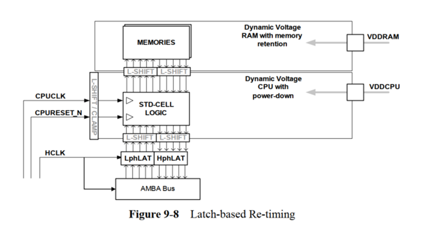
This method requires a CPU clock that is always a multiple of the bus clock (HCLK). We add latches at the interface between the CPU and the AMBA bus. The CPU clock is adjusted so that its rising edge roughly aligns with the activity (rising edge) of the bus clock HCLK. With careful design, we can maintain this relationship within half a CPU clock cycle under all operating conditions (including changes in voltage and clock frequency).
Then we need to handle the fact that the CPU clock may be early or late relative to HCLK. To address the case where the CPU clock is too early, we over-constrain synthesis to ensure that data arrives early (worst-case deviation). If the CPU clock is delayed, the latches ensure that the data is still available.