As the demand for battery life and energy efficiency in electronic devices continues to rise, low power design has become a critical aspect of chip design. The low power design strategies in DFT (Design For Testability) aim to reduce power consumption during both the testing phase and normal operation while ensuring chip test quality and production efficiency.
1. Reasons to Consider Low Power:
The primary goal of reducing power consumption is to extend the usage time of battery-powered electronic products; additionally, low power chips can significantly enhance device reliability and reduce packaging and cooling system costs.
2. Dynamic Power Consumption of Chips in Test Mode
The dynamic power consumption of chips in Test Mode is often several times higher than in Function Mode due to the following reasons:
(1) Test power consumption is related to the logic transition rate. Compared to normal mode, more modules operate in parallel in test mode, resulting in a much higher number of transitions across all nodes. Excessive power consumption can potentially damage the chip;
(2) To improve test quality and reduce test time, high-speed testing (At-speed Test) and parallel testing methods in SoC testing lead to a surge in chip test power consumption;
(3) The integrated DFT logic is off during normal operation but remains active during testing, leading to increased dynamic power consumption;
(4) In scan testing, unnecessary transitions can occur during shift and capture phases;
(5) It can also reduce IR drop. If the IR drop is too large, it can lead to insufficient driving capability during chip testing, resulting in logical errors, which can easily cause missed or false detections, reducing chip yield and production rate by 90.
3. IR Drop
Concept of IR Drop:
IR drop refers to the phenomenon of voltage drop and rise on the power and ground networks in integrated circuits. As semiconductor processes continue to evolve, the width of metal interconnects becomes narrower, and resistance increases (supply voltage also decreases), making the effects of IR drop more pronounced. Therefore, IR drop analysis has become a necessary step in chip signoff. Most industry signoff tools use Redhawk.
Types of IR Drop:
IR drop is mainly divided into two types: static IR drop and dynamic IR drop.
The static IR drop phenomenon is primarily caused by the voltage drop across the metal connections in the power network, which is due to the self-resistance of the metal connections. When current flows through the internal power connections, it causes a voltage drop. Therefore, static IR drop is mainly related to the structure and wiring details of the power network. Thus, static IR drop mainly considers resistance effects, and analyzing the impact of resistance is sufficient.
Dynamic IR drop is the voltage drop caused by current fluctuations when the circuit switches. This phenomenon occurs at the clock’s trigger edge, where the clock edge transition not only activates a large number of transistors but also causes transitions in combinational logic circuits, often generating a large current across the entire chip in a short time, leading to the IR drop phenomenon. The more transistors that switch, the more likely dynamic IR drop will occur.
In the early stages of a project, due to the digital backend implementation database not being ready, post-simulation may not have time to be performed, so dynamic IR drop analysis is generally based on Vectorless. In the later stages of the project, it is necessary to generate corresponding VCD based on a specific scenario, such as max power, and then perform dynamic IR drop analysis based on VCD. Dynamic IR drop analysis based on VCD generally does not require specifying the power values of each submodule; the tool can obtain the corresponding power values from the VCD. If there are no corresponding power values, user-defined values are used.
Impact of IR Drop:
Performance degradation occurs when voltage drops, slowing down the switching speed of gates and reducing performance. Therefore, for high-performance designs, IR drop must be controlled within a very small range. In extreme cases, chip functionality can also be affected. In deep submicron processes, if the power network is not well designed and encounters a very bad case, the IR drop in a specific local area can be particularly large (especially dynamic IR drop), leading to inconsistencies between the STA stage signoff timing and the actual situation (considering OCV still cannot cover design requirements), resulting in setup or hold violations. Setup violations can be mitigated by increasing voltage to enhance frequency (increasing voltage reduces cell delay), but this comes at the cost of increased power consumption, and if dynamic IR drop is not robust enough, the voltage increase may have limited effectiveness. Once hold violations occur, the chip cannot function properly. Therefore, the impact of IR drop is particularly significant in advanced processes and requires high attention from all parties involved.
Methods to Improve IR Drop:
Increase power mesh density, add more power switch cells, and insert enough decap cells (including decoupling capacitance); at the same time, spread out the flipped registers.
4. Low Power Techniques in DFT:
Low power techniques in DFT should include the following three categories: vector-based low power testing techniques, DFT design-based low power testing techniques, and low power test scheduling techniques. Currently, the first two solutions are commonly used in large-scale design projects.
1) Vector-based Low Power Testing Techniques
Test vector transitions can cause state changes in internal nodes of the design, which is the main source of test power consumption. Low power testing methods based on test vectors include low power ATPG, test vector X-filling, test vector reordering, and test input control, such as test point insertion.
Low power ATPG: Create a low_power structure within edt and enable the low_power_shift_enable signal. When generating the pat, open the set_power_control option and report power metrics. You can choose to try_run to attempt to open shift or capture individually or both simultaneously. By observing the ATPG results: changes in the number of patterns; changes in power consumption; changes in coverage. Different designs adopt different options.
The care bits of the test pattern only account for 5%-10% of the total cycles, while unspecified bits are randomly generated as 0/1 for filling. If all bits are filled with 0 or all with 1, the entire scan chain will not toggle in a 0101 pattern, thus reducing power consumption. Our pattern may be a 0101 sequence, which can be adjusted to 0110 to achieve the testing purpose while also reducing the toggle rate.
Vector-based low power testing techniques are relatively easy to implement, generally do not require adding extra logic to the CUT, have minimal impact on the testing process and the performance of the CUT, and have a high degree of dynamic test power optimization. However, these techniques only optimize test power consumption at the test vector level, making it difficult to control static test power consumption. Additionally, due to insufficient consideration of circuit characteristics, the optimization space is relatively limited, making it difficult to play a decisive role in reducing test power consumption; therefore, they are often used as a supplement to other low power techniques.
2) DFT Circuit Design-Based Low Power Testing Techniques
Low power testing techniques based on DFT mainly achieve reduced transitions in scan chains or circuit nodes by adding or modifying DFT logic, thereby reducing test power consumption. This includes toggle suppression, scan_icg_en_control_ip, scan_rst_control_ip, clock tree optimization, scan chain reconstruction, circuit partitioning, and low power BIST.
During the shift period, use AND gates (or OR gates) to prevent the value of SDFF from propagating to combinational logic, thus reducing test power consumption:
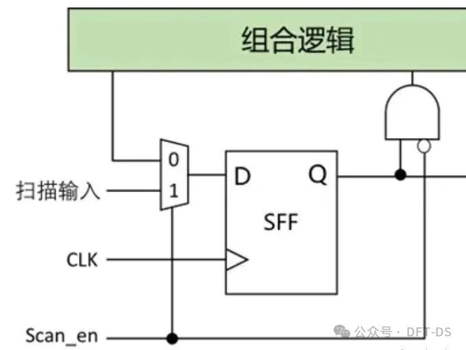
This approach increases the overhead and testing costs of DFT to some extent, may also extend testing time, and have some impact on performance. However, low power design at the circuit level for DFT is highly efficient in optimizing test power consumption and is widely applied in practice.
3) Low Power Test Scheduling Techniques
Parallel testing can reduce SoC testing time, but as the integration of chips increases, the number of embedded IPs in SoC chips continues to grow. The high power and temperature issues brought by parallel testing of various IP cores cannot be ignored, and the limitations of testing access ports and bus resources are insufficient to support parallel testing of all IP cores. Therefore, it is necessary to consider the test scheduling of the SoC system at the full chip level. Generally, different scan modes are used for grouped testing, considering factors such as location and design relationships to plan the WGL.
In MBIST, the step-by-step testing method groups memory during the Memory group phase, and within the same group, step-by-step testing is performed. For example, during step 1 testing, we can turn off the clocks of other parts (controlled by mbist_clk_gate) to reduce dynamic power consumption, and even turn off the power of other parts to further reduce static and dynamic power consumption.
For scan testing: Due to the high capture clock frequency during Transition Fault, power consumption increases sharply, causing MOS parameters to drift, leading to SCAN test failures.
In multi-clock domain designs, a single clock domain chain is generally used, with each clock domain inserting asynchronous OCCs. The other clock domains can be controlled to shut down using occ_kill_clk_en -with_tdr to reduce power.
Step-by-step methods can effectively reduce capture power during SCAN Transition, and since traditional methods do not fully cover test points at the interaction connections between different clock domains, step-by-step methods can also increase test coverage. However, the downside is that the number of test vectors will increase, and testing time will lengthen, leading to increased testing costs. The principle is to use different modes to configure the PLL.
During the shift process, we can reduce power consumption by adding different numbers of buffer cells on the ATE_CLK path, dividing the scan chains into multiple groups so that different scan chains toggle on different rising edges.
During scan testing, capture usually involves the same clock domain’s capture clock toggling simultaneously. Compared to shift, capture uses a high-speed clock, generating significant power consumption in a very short time. To address this issue, we can use empty cycles to separate the capture of the scanning chains, thus reducing instantaneous power consumption.