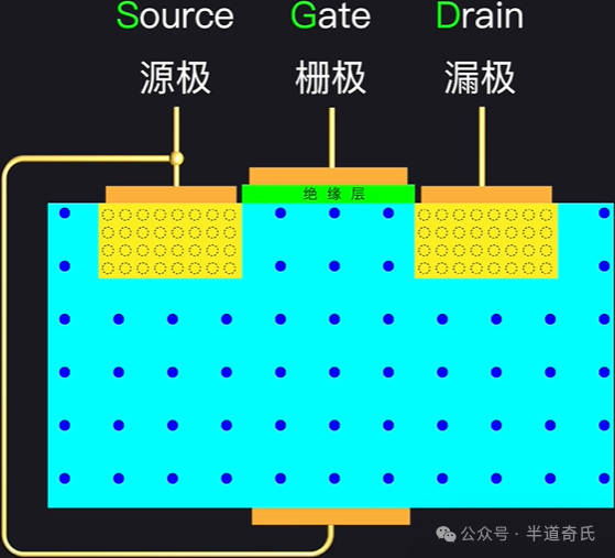
The previous article introduced the PN junction and a typical transistor – the Bipolar Junction Transistor (BJT). Next, we will introduce another typical transistor – the Field Effect Transistor (FET). FET includes Junction Field Effect Transistor (JFET) and Metal-Oxide-Semiconductor Field-Effect Transistor (MOS FET, Metal-Oxide-Semiconductor Field-Effect Transistor, abbreviated as MOS). The specific classification of FET is as follows: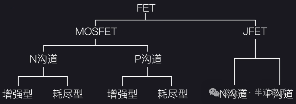 The following will take the enhancement-mode NMOS (N-channel MOS FET) as an example to explain the working principle of MOS. In a P-type semiconductor, two N-type semiconductors are embedded, as shown in the figure:
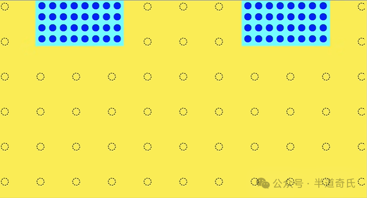 The yellow area represents the P-type semiconductor, and the dashed circle represents holes; the light blue area represents the N-type semiconductor, and the solid blue dots represent electrons. Clearly, at the junction of the P-type and N-type semiconductors, two PN junctions will form, as shown in the following figure:
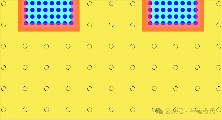 At this point, connecting the two N-type semiconductors with a power supply will result in one side being reverse-biased regardless of the direction of the power supply, and the entire circuit cannot conduct.
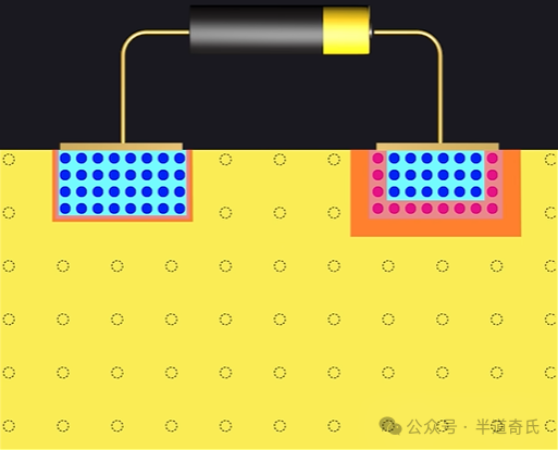 How can we turn on the circuit? As shown in the figure, by covering the P-type semiconductor region between the two N-type semiconductors with an oxide insulating layer, and then adding a layer of metal (with metal, oxide, and semiconductor combined), we can connect the two ends with a power supply.
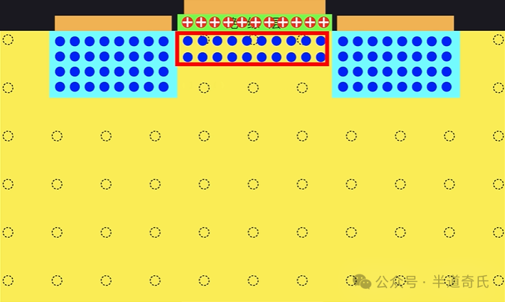
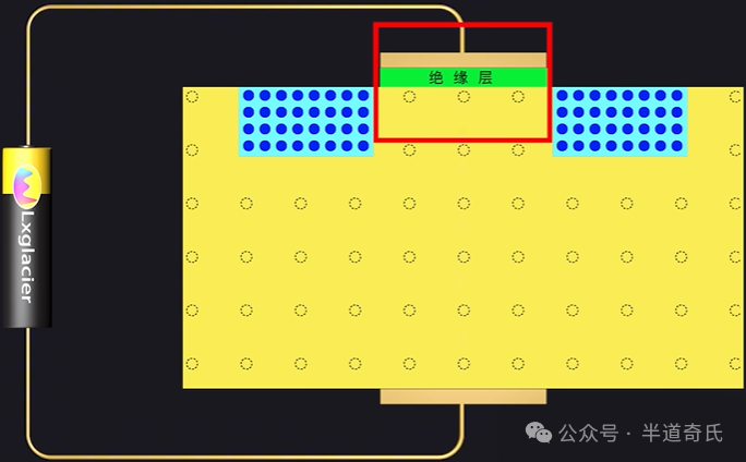 The red box part in the middle, due to the barrier of the insulator, acts like a capacitor. Although there is no current, a large amount of positive and negative charges accumulate on both sides of the insulating layer, as shown in the following figure:
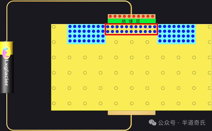 At this time, since the accumulation of electrons exceeds the number of holes (minority carriers), the red box area can be equivalently regarded as an N-type semiconductor (inversion layer, semiconductor type inverted), forming an N-channel, as shown in the following figure:
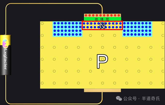 At this point, as shown in the following figure, the two sides of the N-type semiconductors are connected by the N-channel, and the circuit connecting both sides is naturally conducting.
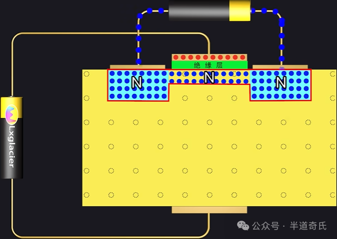 To increase the conduction current, the channel needs to be enlarged, which can be achieved by increasing the voltage of the control circuit. It can be seen that the MOS control circuit controls the conduction current through voltage, and the control circuit itself does not carry current, which is fundamentally different from the BJT that controls a large current with a small current. This is also the reason why MOS is called a field-effect transistor. MOS has a source, gate, and drain, which correspond to the emitter, base, and collector of a BJT.
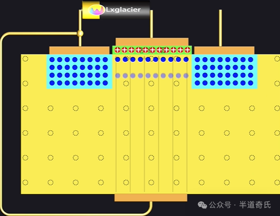
 The enhancement-mode PMOS is simply the exchange of the above N-type and P-type semiconductors, turning the N-channel into a P-channel. The depletion-mode NMOS injects positive charges (removing electrons) into the insulating material of the enhancement-mode NMOS, making it positively charged. The free electrons (minority carriers) in the P-type semiconductor are attracted and gathered, resulting in the formation of an N-channel in the red box area, as shown in the following figure. At this time, the control circuit does not apply voltage, and the main circuit is conducting.
 When the control circuit applies voltage, like charges repel and push the accumulated electrons to “deplete” them, causing the main circuit to disconnect, as shown in the following figure.
 The depletion-mode PMOS is the exchange of the N-type and P-type semiconductors in the above figure, with electrons injected into the insulating layer carrying a negative charge. Compared to BJTs, MOS transistors have characteristics of high-density integration, low power consumption, and ease of large-scale production, making them the main type of transistor used in modern integrated circuits. Future plans will introduce how transistors form integrated circuits. The text is self-organized and written, and the images are sourced from the internet.