Some basic concepts about ARM, you can refer to my previous article:
“What Exactly Are Cortex, ARMv8, ARM Architecture, ARM Instruction Set, SoC? A Comprehensive Guide to Basic Concepts【Popular Science】”
For the IDE development environment used for ARM instructions, you can refer to the following article:
“1. Learn ARM from Scratch – Installing Keil MDK uVision Integrated Development Environment”
“2. Learn ARM from Scratch – CPU Principles, Explanation Based on ARM SoC”
With the principles of computer hardware architecture, I can now learn basic knowledge such as ARM modes, registers, and pipelines.
1. ARM Technical Features
The success of ARM is attributed to its unique corporate operation model on one hand, and of course, the excellent performance of ARM processors on the other. As an advanced RISC processor, ARM processors have the following characteristics.
-
Small size, low power consumption, low cost, and high performance. -
Supports Thumb (16-bit) / ARM (32-bit) dual instruction sets, and is well compatible with 8-bit / 16-bit devices. -
Heavily uses registers, leading to faster instruction execution speeds. -
Most data operations are performed in registers. -
Flexible and simple addressing modes, with high execution efficiency. -
Fixed instruction length.
2. Basic Data Types of ARM
ARM adopts a 32-bit architecture, and the basic data types of ARM are as follows:
-
Byte: 8 bits. -
Halfword: 16 bits (halfword must be aligned to a 2-byte boundary). -
Word: 32 bits (word must be aligned to a 4-byte boundary). Memory can be viewed as a linear byte array with indices ranging from 0 to 2^32-1. Each byte has a unique address.
Note:
-
ARM architecture versions above v4 support the above 3 data types, while versions before v4 only support bytes and words.
-
When any of these data types is declared as unsigned, the n-bit data value represents a range of non-negative numbers from 0 to 2^n-1, typically using binary format.
-
When any of these data types is declared as signed, the n-bit data value represents a range of integers from -2^(n-1) to 2^(n-1)-1, using binary’s two’s complement format.
-
All data type instruction operands are of word type, such as the operand “0x1” in “ADD r1,r0,#0x1” is processed as word type data.
-
Load/Store data transfer instructions can access and transfer data from memory, which can be bytes, halfwords, or words. During loading, zero-extension or sign-extension for bytes or halfwords is performed automatically. The corresponding instructions are LDR/STRB (byte operation), LDRH/STRH (halfword operation), LDR/STR (word operation).
-
ARM instructions compile to 4 bytes (aligned with word boundary); Thumb instructions compile to 2 bytes (aligned with halfword boundary).
3. ARM Processor Operating Modes
There are a total of 7 operating modes for ARM processors prior to the Cortex series.
1. Operating Modes
The ARM processors of the Cortex series have 8 operating modes, with an additional monitor mode, as shown in the figure below:
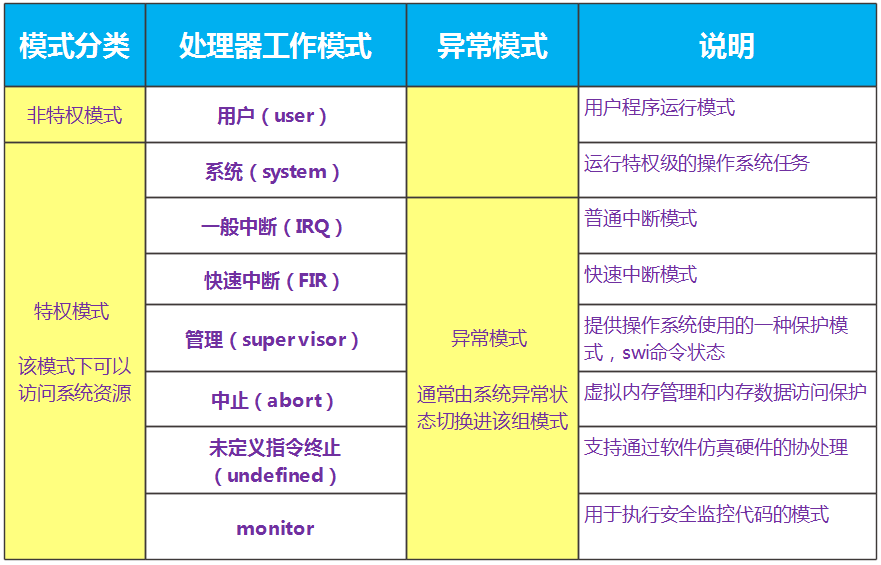
The reason for designing so many modes is to “handle various unexpected events during CPU operation”, such as supporting the normal operation of application programs, while many exceptions may occur at any point in time, such as shutdown, receiving network card information, division by zero, accessing illegal memory, parsing illegal instructions, etc. Not only must these exceptions be handled, but the system must also be able to return from exceptions to continue executing the original program.
-
User Mode: User mode is the working mode of user programs, running in the user state of the operating system. It does not have permission to operate other hardware resources, can only process its own data, and cannot switch to other modes. To access hardware resources or switch to other modes, it can only do so through software interrupts or exceptions. -
System Mode: System mode is a privileged mode, not limited by user mode. User mode and system mode share a set of registers, making it convenient for the operating system to access user mode registers in this mode, and some privileged tasks of the operating system can use this mode to access controlled resources. -
General Interrupt Mode: General interrupt mode, also known as normal interrupt mode, is used to handle general interrupt requests, and is automatically entered after hardware generates an interrupt signal. This mode is a privileged mode and can freely access system hardware resources. -
Fast Interrupt Mode: Fast interrupt mode is relative to general interrupt mode, used to handle urgent interrupt requests, mainly for high-speed data transmission and channel processing. -
Manager Mode: Manager mode is the “default mode after CPU power on”, primarily used for system initialization, and software interrupt handling also occurs in this mode. When a user program in user mode requests to use hardware resources, it enters this mode through software interrupt. -
Abort Mode: Abort mode is used to support virtual memory or memory protection. When a user program accesses an illegal address or a memory address without permission to read, it enters this mode. The segment fault that often occurs in Linux programming usually throws a return in this mode. -
Undefined Mode: Undefined mode is used to support software emulation of hardware coprocessors. When the CPU cannot recognize an instruction operation during the instruction decoding phase, it enters undefined mode. -
Monitor: An extended mode for executing security monitoring code for safety; it is also a privileged mode.
Except for user mode, the remaining 6 modes are referred to as non-user modes or privileged modes; among them, the 5 modes other than user mode and system mode are called exception modes, commonly used for handling interrupts or exceptions, as well as accessing protected system resources.
2. Mode Switching
The ARM microprocessor’s operating mode can be changed by software, as well as by external interrupts or exception handling. Application programs run in user mode, and when the processor operates in user mode, certain protected system resources cannot be accessed.
3. Exceptions
Exceptions are caused by the processor executing instructions that lead to the original running program’s termination. Exceptions are related to instruction execution, are generated by the CPU executing the program, are synchronous, and can be divided into precise exceptions and imprecise exceptions. Exception handling follows strict program order and cannot be nested; only after the first exception handling is completed and returns can subsequent exceptions be processed.
4. Exception Sources
To enter exception mode, there must be an exception source. ARM specifies 7 types of exception sources:
| Exception Source | Description |
|---|---|
| Reset | Executed during power on |
| Undef | Executed when an illegal instruction in the pipeline reaches the execution state |
| SWI | Executed when a software interrupt instruction is completed |
| Prefetch | Executed when an instruction is prefetched from memory and fails for some reason; this exception occurs only if it reaches the execution state |
| Data | If a prefetch instruction attempts to access an illegal memory unit, this exception occurs |
| IRQ | Normal interrupt |
| FIQ | Fast interrupt |
5. Relationship Between Exception Sources and Modes
-
Reset exception enters manager mode; -
Fast interrupt request exception enters fast interrupt mode, supporting high-speed data transmission and channel processing (FIQ exception response enters this mode); -
Interrupt request exception enters interrupt mode, used for general interrupt processing (IRQ exception response enters this mode); -
Prefetch abort and data abort exceptions enter abort mode, used to support virtual memory and/or memory protection; -
Undefined instruction exception enters undefined mode, supporting software emulation of hardware coprocessors (undefined instruction exception response enters this mode); -
Software interrupt and reset exceptions enter manager mode, operating system protection code (system reset and software interrupt response enters this mode);
After an exception occurs, the CPU must respond immediately, and exceptions will be explained in detail later.
4. ARM Registers
The Cortex A series ARM processors have a total of 40 32-bit registers, of which 33 are general-purpose registers and 7 are status registers. User mode and system mode share the same set of registers.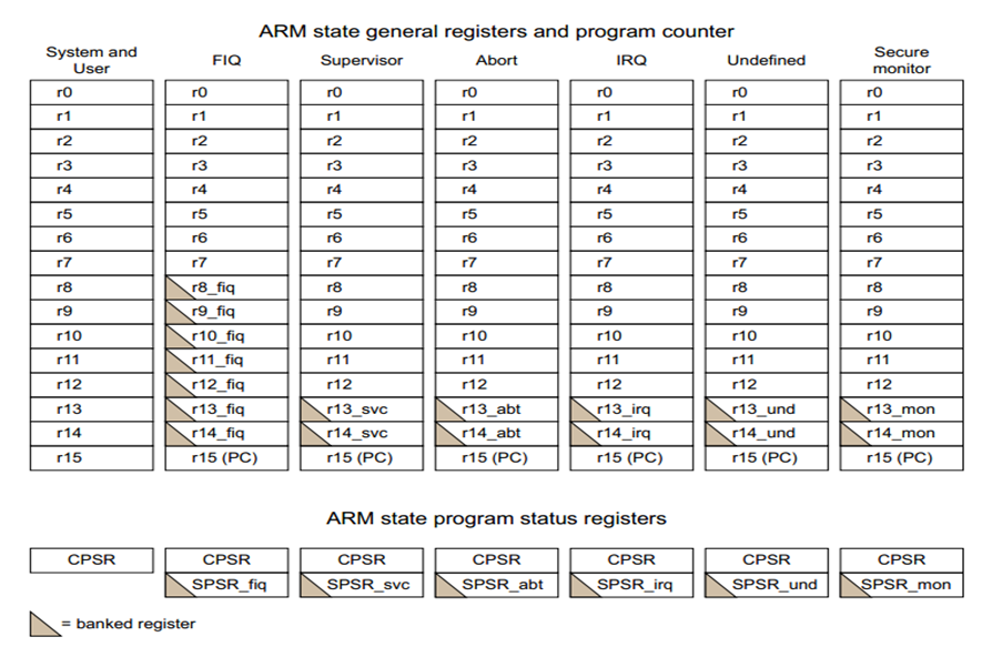 The general-purpose registers include R0~R15 and can be divided into 3 categories:
-
Ungrouped registers R0~R7 -
Grouped registers R8~R14, R13 (SP), R14 (LR) -
Program Counter PC (R15), R8_fiq-R12_fiq are unique to fast interrupts
1. Ungrouped Registers R0~R7
In all operating modes, ungrouped registers point to the same physical register; they are not used by the system for special purposes. Therefore, during interrupt or exception handling, when switching operating modes, the same physical registers are used across different processor operating modes, which may lead to data corruption in the registers.
2. Grouped Registers R8~R14
For grouped registers, each accessed physical register is related to the current running mode of the processor.
For R8~R12, each register corresponds to 2 different physical registers; when using FIQ (fast interrupt mode), the registers R8_fiq~R12_fiq are accessed; when using other modes except FIQ, the registers R8_usr~R12_usr are accessed.
For R13 and R14, each register corresponds to 7 different physical registers, one of which is shared between user mode and system mode, while the other 6 physical registers correspond to the other 6 different operating modes, and the following notation is used to distinguish different physical registers:
R13_mode R14_mode
Where mode can be: “usr, fiq, irq, svc, abt, und, mon”.
3. Register R13 (SP)
In ARM instructions, it is often used as a “stack pointer”; users can also use other registers as stack pointers, but in the Thumb instruction set, some instructions strictly require the use of R13 as the stack pointer.
Register R13 is often used as a stack pointer in ARM instructions, but this is merely a convention; users can also use other registers as stack pointers. In the Thumb instruction set, however, certain instructions strictly require using R13 as the stack pointer.
Since each operating mode of the processor has its own independent physical register R13, during the initialization part of user applications, R13 for each mode is usually initialized to point to the stack space of that operating mode. This way, when the program enters exception mode, the registers that need protection can be placed onto the stack pointed to by R13, and when the program returns from exception mode, it can restore from the corresponding stack, ensuring the normal execution of the program after an exception occurs.
4. R14 (LR) Link Register
When executing subroutine call instructions (BL), R14 can obtain a backup of R15 (Program Counter PC).
In each operating mode, R14 can be used to save the return address of subroutines. When calling a subroutine with the BL or BLX instruction, the current value of PC is copied to R14, and after executing the subroutine, the value of R14 is copied back to PC to complete the subroutine return. The above description can be achieved using instructions.
Returning from a Subroutine:
“Method 1:”
  MOV PC, LR
or
  BX LR
“Method 2:” At the entry of the subroutine, use the following instruction to store R14 onto the stack:
STMFD SP!,{LR}
Correspondingly, the following instruction can complete the subroutine return:
LDMFD SP!,{PC}
5. R15 (PC) Program Status Register
Register R15 serves as the Program Counter (PC). In ARM state, bits [1:0] are 0, and bits [31:2] are used to store PC; in Thumb state, bit [0] is 0, and bits [31:1] are used to store PC.
For example, if the value of PC is 0x40008001, then during addressing, it will actually look up address 0x40008000, automatically ignoring the low 2 bits. “The reason for this, the readers should think for themselves?”
Due to the multi-stage pipeline technology adopted by the ARM architecture, for the ARM instruction set, PC always points to the address of the next two instructions, meaning the value of PC is the current instruction’s address plus 8 bytes.
Thus: PC value = current program execution position + 8
[Pipeline technology reference in Chapter 7]
6. CPSR, SPSR
“CPSR” (Current Program Status Register) can be accessed in any operating mode. It includes condition flags, interrupt disable bits, current processor mode flags, and other related control and status bits.
Each operating mode also has a dedicated physical status register called “SPSR” (Saved Program Status Register). When an exception occurs, SPSR is used to save the current value of CPSR, and upon exiting the exception, SPSR can be used to restore CPSR.
Since user mode and system mode do not belong to exception modes, they do not have SPSR. Accessing SPSR in these two modes results in undefined behavior.
The format of register CPSR is as follows:
-
Condition code flags “N, Z, C, V” are condition code flag bits that can be changed by the results of arithmetic or logical operations and can determine whether a certain instruction is executed. In ARM state, the vast majority of instructions are conditionally executed, while in Thumb state, only branch instructions are conditionally executed.
“N (Number)”: When performing operations with two’s complement signed numbers, N=1 indicates the result is negative, N=0 indicates the result is positive or zero.
“Z (Zero)”: Z=1 indicates the result is zero, Z=0 indicates the result is non-zero.
“C”: C can be set in 4 ways:
-
(Come) Addition operations (including CMP): When a carry is generated during the operation, C=1; otherwise, C=0. -
Subtraction operations (including CMP): When a borrow occurs, C=0; otherwise, C=1. -
For non-addition/subtraction instructions that include shift operations, C is the last bit shifted out. -
For other non-addition/subtraction instructions, C’s value usually remains unchanged.
“V” (oVerflow): For addition/subtraction operation instructions, when the operands and results overflow in binary’s two’s complement representation, V=1 indicates overflow in the sign bit; for other non-addition/subtraction instructions, V’s value usually remains unchanged.
“Q”: In ARM V5 and above versions of E series processors, the Q flag indicates whether enhanced DSP operation instructions overflow. In other versions of processors, the Q flag is undefined.
“J:” Only ARM v5TE-J architecture supports, T=0; J=1 indicates the processor is in Jazelle state, which can also combine with other bits.
“E bit:” Endian control bit.
“A bit:” A=1 prohibits inexact data exceptions.
“T:” T=0; J=0 indicates the processor is in ARM state; T=1; J=0 indicates the processor is in Thumb state; T=1; J=1 indicates the processor is in ThumbEE state.
-
Control bits
| bit | Mode | Registers accessible in ARM mode |
|---|---|---|
| 0b10000 | User mode | PC, CPSR, R0~R14 |
| 0b10001 | FIQ mode | PC, CPSR, SPSR_fiq, R14_fiq~R8_fiq, R0~R7 |
| 0b10010 | IRQ mode | PC, CPSR, SPSR_irq, R14_irq~R13_irq, R0~R12 |
| 0b10011 | Manager mode | PC, CPSR, SPSR_svc, R14_svc~R13_svc, R0~R12 |
| 0b10111 | Abort mode | PC, CPSR, SPSR_abt, R14_abt~R13_abt, R0~R12 |
| 0b11011 | Undefined mode | C, CPSR, SPSR_und, R14_und~R13_und, R0~R12 |
| 0b11111 | System mode | PC, CPSR, R0~R14 |
Note the characteristics of these 5 bits: the highest bit is always 1, while the low 4 bits have different values. This is very important; to understand the source code of uboot and Linux, especially the code for exception handling, you must know the values of these bits.
5. Coprocessors
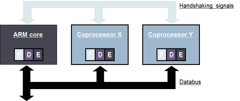 The ARM architecture allows for the extension of the instruction set by adding coprocessors. The most commonly used coprocessors are system coprocessors for controlling on-chip functions.
For example, the CP15 coprocessor controls cache and memory management units (MMU), and the mcr instruction sets the exception vector table address.
ARM supports 16 coprocessors, and during program execution, each coprocessor ignores instructions belonging to the ARM processor and other coprocessors. When a coprocessor hardware cannot execute its corresponding instructions, an undefined exception interrupt will occur. In the exception interrupt handler, software can simulate the hardware’s operations, such as if the system does not include a vector floating-point processor, a floating-point software simulation package can be chosen to support vector floating-point operations.
ARM coprocessor instructions include the following three categories:
-
Data operation instructions for initializing ARM coprocessors -
Data transfer operations between ARM processor registers and ARM coprocessor registers -
Data transfer between ARM coprocessor registers and memory units
We only need to know a few commonly used coprocessor instructions, which will be mentioned in later articles.
6. Jazelle
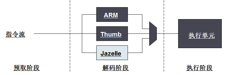 Jazelle is a state added to run the Java virtual machine.
ARM’s Jazelle technology provides hardware support for Java bytecode, greatly improving system performance.
Since the ARM architecture is 32-bits, 16-bits = “halfword”, and “word” = 32-bits.
Java bytecode is the instruction set of an independent 8-bits architecture. Jazelle executes most bytecode in hardware (while others use highly optimized ARM code). This is due to a trade-off between hardware complexity (power consumption & chip area) and speed.
7. Instruction Pipeline
Pipeline technology shortens program execution time by allowing multiple functional components to work in parallel, improving the efficiency and throughput of processor cores, making it one of the most important technologies in microprocessor design.
1. 3-Stage Pipeline
Up to the ARM7, ARM processors use a simple 3-stage pipeline, which includes the following pipeline stages: (1) Instruction Fetch: Load an instruction from the register. (2) Decode: Identify the instruction to be executed and prepare control signals for the data path in the next cycle. In this stage, the instruction occupies the decoding logic without occupying the data path. (3) Execute: Process the instruction and write the result back to the register.
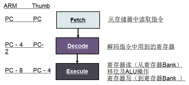 When the processor executes simple data processing instructions, the pipeline allows an average of one instruction to be completed per clock cycle. However, one instruction requires 3 clock cycles to complete, leading to a 3-cycle delay, but the throughput is one instruction per cycle.
For a 3-stage pipeline, the value in the PC register is not the address of the instruction being executed, but the address of the prefetched instruction. This knowledge is crucial, and we will provide detailed examples later to prove it.
To meet high-performance requirements, the processor’s organizational structure needs to be reconsidered. The main methods to improve performance are:
-
Increase clock frequency. Increasing clock frequency necessarily shortens the instruction execution cycle, so it requires simplifying the logic of each pipeline stage and increasing the number of pipeline stages. -
Reduce the average instruction cycle count (CPI) per instruction. This requires reconsidering the implementation method of more than one pipeline cycle in the 3-stage pipeline ARM to occupy fewer cycles, or reducing pipeline stalls caused by instruction dependencies, or combining both approaches.
Higher performance ARM cores use a 5-stage pipeline and have separate instruction and data memory. The Cortex-A8 has a 13-stage pipeline, but ARM has not disclosed any relevant details regarding the technology.
From the classic ARM series to the current Cortex series, the structure of ARM processors has evolved towards complexity, but what has not changed is the CPU’s addressing instructions and address relationships, “regardless of how many pipeline stages there are, the current PC position can be judged according to the original 3-stage pipeline operation characteristics.”
2. Pipeline Examples
For better understanding, let’s take the 3-stage pipeline as an example.
1) Optimal Pipeline
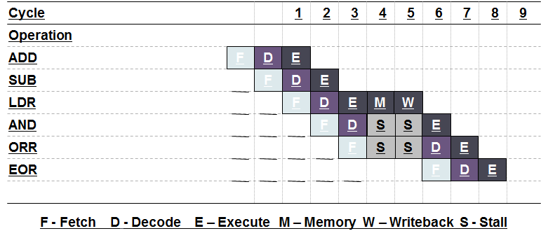
This is an ideal case where all instructions are executed in registers, and the processor does not need to leave the chip. In each cycle, one instruction is executed, and the pipeline capacity is fully utilized. Instruction cycle count (CPI) = 1.
2) LDR Pipeline
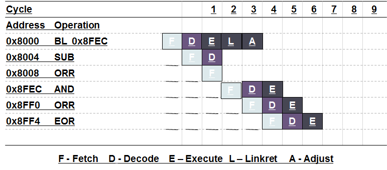
In this case, 4 instructions are executed in 6 cycles. Instruction cycle count (CPI) = 1.5.
Unlike the optimal pipeline, the loading (LDR) operation moves data into the chip, causing the instruction/data bus to be occupied, hence followed by an internal write-back cycle to complete the data write back to the register.
-
The data bus is used in cycles 1, 2, and 3; cycle 6 is instruction fetch, cycle 4 is data load, and cycle 5 is an internal cycle to complete the data write back to the register. -
Cycle 3 is the execution cycle: generating address. -
Cycle 4 is the data cycle: fetching data from memory (data appears in the core only at the end of cycle 4). -
Cycle 5 is the write-back cycle: writing data back to the register bank through the data channel’s B bus and ALU. -
Cycle 6’s execution is delayed until cycle 5’s write-back is complete (using ALU). Similarly, internal cycles do not need to wait for the status, but reading/writing memory might require it.
3) Branch Pipeline
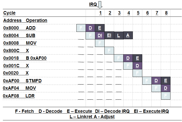
BL instruction is used to implement a jump in the instruction flow and store the return address in register R14 (LR).
-
The branch instruction calculates the destination of the branch in its first cycle while completing an instruction prefetch at the current PC. The pipeline is blocked. This prefetch must be done in any case because it is too late to stop prefetching when the decision address is generated. -
The second cycle completes the instruction fetch from the branch target address, while the return address is stored in R14 if the link bit is set. -
The third cycle completes the instruction fetch of the target address +4, refilling the pipeline, and if the jump is linked, R14 is adjusted (subtracting 4) for a simple return. -
The branch takes three clock cycles to execute BL, followed by adjustment phases.
4) Interrupt Pipeline
“The minimum response time for IRQ interrupts = 7 cycles”
-
Cycle 1: The core is informed of an interrupt. IRQ will not be responded to until the current instruction is completed (MUL and LDM/STM instructions will have long delays). Decode stage: The interrupt is decoded (the interrupt is enabled, and the corresponding flags are set…). If the interrupt is enabled and serviced, normal instructions will not be decoded.
-
Cycle 2: At this point, it always enters ARM state. Execute the interrupt (fetch the address of the IR vector), save CPSR to SPSR, change CPSR mode to IRQ mode, and disable further IRQ interrupt inputs.
-
Cycle 3: Save PC (0x800C) to r14_irq, fetch the instruction from the IRQ exception handling vector.
-
Cycle 4: Decode the instruction in the vector table; adjust r14_irq to 0x8008.
-
Cycles 4 and 5: No useful instruction fetch, due to the jump in cycle 6.
-
Cycle 6: Fetch the first instruction of the exception handling subroutine; return from subroutine:
SUBS pc, lr
This will restore the working mode and fetch the instruction from the next instruction after responding to the interrupt. If there are multiple interrupts, the return address must be saved on the stack. Note that the maximum FIQ response delay is 29 cycles (not 28 cycles in Thumb state!).

Summary of Learning ARM from Scratch Series

1. 0. What Exactly Are Cortex, ARMv8, ARM Architecture, ARM Instruction Set, SoC? A Comprehensive Guide to Basic Concepts【Popular Science】
2. 1. Learn ARM from Scratch – Installing Keil MDK uVision Integrated Development Environment
3. 2. Learn ARM from Scratch – CPU Principles, Explanation Based on ARM SoC
Recommended Reading
To join the group, please add WeChat account of Yikoujun, guiding you to get started with embedded systems.
Click “Read Original” for more shares, and welcome to share, collect, like, and view.