With the rapid development of fields such as Artificial Intelligence (AI) and High-Performance Computing (HPC), the demand for chip performance is increasing. In this context, glass substrate technology, with its superior physical properties and advanced packaging potential, is gradually becoming the new favorite in the semiconductor industry. The strong promotion by the U.S. government, particularly the recent announcement of funding for companies like Absolics through the CHIPS Act, marks an unprecedented development opportunity for the glass substrate industry.
In the past two years, the continuous maturation of glass substrate technology has gradually revealed its potential in advanced packaging. Major global semiconductor companies, such as Intel and Samsung, are actively laying out glass substrate technology. Intel announced plans for mass production of glass substrates by 2030 and has invested $1 billion in its Arizona plant to establish a research and development line and supply chain for glass substrates. Samsung has formed a united front with Samsung Electronics, Samsung Display, and Samsung Electro-Mechanics to enter the glass substrate R&D field. Furthermore, glass substrate materials have a wide range of applications, including replacing CoWoS interposer/FC-BGA substrates, co-packaging optical device integration, Mini/Micro LED backplane materials, passive devices, and sensor packaging. Today, more leading companies, including BOE and TSMC, are actively exploring glass substrate technology.
Through an in-depth analysis of recent patents related to glass interposers and core substrates in advanced packaging, one can glimpse the current research hotspots and development directions in the field of glass substrates.
1. Patent Landscape of Glass Substrates
According to statistics from Knowmade, there are currently over 300 patents related to glass interposers and glass core substrates used in advanced packaging, with major participants including Intel and Absolics. These two companies together hold nearly half of the patents, while more than 70 other entities collectively hold over 150 patents.
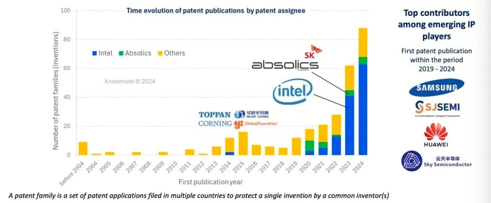
Intel: Leads in the number of patents, holding the most patent applications, with a portfolio covering glass core substrates and glass interposers, showcasing a comprehensive and balanced layout, placing it at the forefront of technological innovation in the industry.
Absolics: Focused on the glass core substrate field, is Intel’s closest competitor in terms of patent quantity, highlighting its R&D investment and technological strength in this specific area.
Numerous other entities: Over 70 entities collectively hold half of all relevant patents, but each entity holds relatively few patents, indicating a highly fragmented situation. This includes TOPPAN, Corning, Hitachi, GlobalFoundries, TSMC, Samsung, Qualcomm, Unimicron, BOE, Huajin Semiconductor, Xiamen Yuntian, Shenghe Jingwei, Tongfu Microelectronics, and Guangdong Fozhi Semiconductor, among others, which also occupy a certain share in the patent layout of the glass substrate industry. From the trend of patent applications, Intel was proactive in its layout early on, continuously accumulating patents since 2004, but has seen a surge in recent years. From 2019 to 2024, many companies have entered the fray, such as Absolics (SK Group) increasing its patent applications, while Samsung and China’s Shenghe Jingwei and Xiamen Yuntian Semiconductor have emerged during this period.
This indicates that the technological innovation and intellectual property competition in the glass substrate industry are becoming increasingly fierce, attracting more and more enterprises’ attention and investment.
Among the emerging competitors, Samsung, Shenghe Jingwei, and Xiamen Yuntian Semiconductor have published numerous patents for the first time between 2019 and 2024, showing an upward trend year by year, marking their active exploration and innovative achievements in glass substrate technology R&D, and continuously increasing R&D investment, further enriching the technological innovation ecosystem of the industry and pushing the patent competition landscape of the entire industry towards diversification.
From a regional distribution perspective, the leading companies Intel and Absolics have a wide geographical coverage in their patent layouts, applying for patents in the U.S., mainland China, Taiwan, South Korea, Japan, and Europe. This global patent layout strategy helps them protect their technological innovations in different markets and also reflects the international competitive landscape of the glass substrate industry.
Samsung mainly applies for patents in the U.S., China, and South Korea, focusing on its technological protection and market competitive advantages in the Asian and North American markets.
Domestic enterprises have varying strategies, with some focusing on both domestic and international layouts, while others concentrate on domestic layouts. For example, Shenghe Jingwei’s patent applications are concentrated in the U.S. and China, reflecting its emphasis on these two important markets and its strategic layout in local market competition. Meanwhile, Xiamen Yuntian currently has almost all of its patent applications in China, indicating its gradual accumulation of technological strength and intellectual property assets based on its local market foundation, laying the groundwork for future expansion into broader markets.
2. Research Hotspots in Glass Substrate Technology
– Integration of Glass Substrates and Interposers in Packaging
Transitioning from silicon materials to glass materials involves addressing multiple challenges, which are also reflected in patent applications. This includes achieving thinner packaging in embedded chips; higher density interconnections for chip-to-chip coupling; hybrid bonding of chips and glass; and Intel’s research on EMIB, among others.
Among these, innovations in metallization and connection technology are one of the research hotspots. For example, high aspect ratio via (TGV) metallization: developing efficient metallization processes targeting the high aspect ratio characteristics of TGV to ensure uniform metal filling inside the vias, free of voids, improving electrical connectivity and reducing signal transmission losses; enhancing metal/glass adhesion: studying the adhesion mechanism between metal and glass through surface treatment or material improvement methods to strengthen the bond between the two, preventing delamination or peeling during the packaging process or product use, thus improving long-term reliability; hybrid bonding technology (chip/glass): exploring hybrid bonding methods between chips and glass, such as direct Cu/SiO₂ bonding, achieving tighter connections, increasing packaging density, reducing signal delay, while optimizing thermal management performance, providing solutions for high-performance computing and high-density packaging.
Optimizing packaging architecture and enhancing functionality is another major hotspot. For instance, embedded chips (Embedded Die): achieving thinner packaging structures by embedding chips in glass substrates, reducing packaging volume and increasing product integration to meet the miniaturization and lightweight trends of electronic products; chip-to-chip coupling (D2D Coupling): focusing on enhancing connectivity between chips, developing high-density, high-performance interconnection technologies, such as using micro bumps (µbumps) or interconnect bridges to achieve faster and more stable data transmission, enhancing overall system performance; Intel has been researching Fan-out Embedded Glass Bridge (EMIB) technology for years: studying the application of EMIB technology on glass substrates, achieving efficient signal transmission between chips by embedding conductive bridges in glass substrates, while optimizing the heat dissipation performance of the packaging, improving product reliability and performance.
Additionally, co-packaging photonics is also a research hotspot, with half of Intel’s patent portfolio focusing on photonic integration-related fields. There are also patents related to cost-effective large-size panel-level packaging and thermal management.
– Manufacturing Processes or Designs of Glass Substrates and Interposers
Patents related to the design and manufacturing of glass substrates and glass interposers mainly involve defect control (materials or procedures for quality inspection); reinforcement methods for thin glass substrates; alignment methods (based on glass transparency); metallization of high AR vias, adhesion between metal and glass; TGV structure and manufacturing; reducing signal crosstalk within interposers; thermal management, etc.
Among these, improvements in manufacturing processes are a research hotspot. This includes innovations in surface treatment technology: developing new surface treatment processes targeting the roughness of glass surfaces and the challenges posed by TGV’s high aspect ratio, such as directly plating copper on dielectrics (without a seed layer), achieving void-free metal via filling, improving metallization quality and reliability. At the same time, researching technologies like plasma surface activation to enhance the reactivity of glass surfaces with metals, improving adhesion performance; stress management and warpage control: addressing stress issues in glass substrates during manufacturing and usage by optimizing manufacturing process parameters or adopting special structural designs to reduce the risk of warpage. For example, forming cavities in glass core substrates and embedding silicon bridge interposers, utilizing the material characteristics of glass and silicon to effectively reduce the degree of warpage of the packaging substrate, improving product flatness and stability; pre-fabricated components and simplified assembly processes: developing pre-fabricated copper pillar components and exploring efficient assembly methods with glass materials, such as manufacturing copper pillars on silicon substrates through electrochemical deposition and then anodically bonding them with glass substrates, avoiding complex and expensive electroplating and chemical mechanical polishing (CMP) steps, while integrating a passivation layer as a stress buffer layer to enhance product reliability and reduce production costs.
Thermal management and optical performance optimization are another major hotspot. For instance, designing glass core substrates with fluid channels for effective cooling through the packaging substrate, rather than solely relying on top chip heat dissipation, improving heat dissipation efficiency and ensuring product stability under high-power operating conditions. Meanwhile, researching designs like thermal conductive sleeves around TGVs to improve thermal conduction pathways, avoiding crack propagation around vias due to mismatched thermal expansion coefficients (CTE) between glass and copper, enhancing product thermal reliability. In terms of optical performance, leveraging the optical transparency of glass to optimize the optical design of glass substrates, such as developing waveguide integration technology for efficient integration of photonic integrated circuits (PIC) and electronic chips (EIC) on glass substrates, improving optical signal transmission efficiency and accuracy, providing better platform support for photonic applications.
3. Key Technical Challenges and Corresponding Patent Solutions
– Mechanical Stress Management (Warpage Issues)
The large difference in thermal expansion coefficients between glass materials and other packaging materials (such as silicon chips, organic packaging materials, etc.) can cause uneven thermal expansion or contraction during temperature changes in the packaging process, leading to warpage deformation of the packaging substrate. Warpage issues not only affect packaging precision and electrical connectivity but can also lead to fatigue and cracking of solder joints between chips and substrates, severely impacting product reliability and lifespan.
Patent Solutions
Composite structural design: Samsung’s patent (e.g., CN118431173) involves the composite structural design of glass substrates and glass interposers. By optimizing the combination between the two, utilizing the low CTE and high rigidity characteristics of glass, it effectively reduces the warpage degree of the packaging substrate.
Application of cavities and embedded structures: forming cavities in glass core substrates and embedding silicon bridge interposers and other components. This structural design can compensate for the thermal expansion differences between different materials to some extent, adjusting the stress distribution within the structure to reduce the risk of warpage deformation, thus enhancing the stability and reliability of the packaging structure.
– Glass Surface Treatment
The high roughness of glass surfaces and the high aspect ratio of TGV pose difficulties for the metallization process, making it challenging to achieve uniform, void-free metal deposition on such surfaces, thereby affecting electrical connectivity. Smooth glass surfaces exhibit poor adhesion, and when combined with metal layers (such as copper), they are prone to delamination or peeling, reducing the reliability of the packaging structure. Additionally, during the packaging process, the movement of glass substrates in processing equipment can also lead to handling difficulties due to adhesion issues.
Patent Solutions
Direct copper plating process innovation: Intel’s patent (US20240213131) proposes a process for directly plating copper on dielectrics without a seed layer. By ionizing the -OH bonds formed on the glass surface to create -O⁻ bonds, which have high reactivity with metal ions, direct copper plating is achieved, effectively solving the conformal metallization issue under the high aspect ratio of TGV and avoiding potential voids in traditional processes, thus improving metallization quality.
Surface roughening to enhance adhesion: Another Intel patent (US20240222249) involves roughening the surface of glass core layers. Roughened glass surfaces can increase the mechanical interlocking force with metal layers, thereby enhancing adhesion between glass and metal, addressing the separation issues between glass and copper features caused by adhesion problems, and improving stability and reliability in processing.
– Thermal Management
As the performance of electronic products improves and chip power consumption increases, the heat dissipation issues of glass substrates in packaging become a key challenge. Glass itself has relatively poor thermal conductivity, making it crucial to effectively dissipate heat generated by chips to ensure product stability under high-temperature conditions. In glass core substrates or glass interposers, the mismatch of thermal expansion coefficients (CTE) between materials, such as between glass and copper (commonly used for via filling and circuit connections), can easily generate thermal stress during temperature changes, potentially leading to via cracking and delamination issues between chips and substrates, affecting reliability.
Patent Solutions
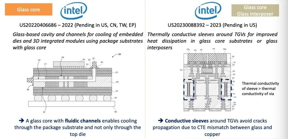
Glass-based cooling structural design: Intel proposed a cavity and channel structure based on glass (e.g., US20220406686) for cooling embedded chips and 3D integrated modules. By designing fluid channels within the glass core substrate, cooling media can flow through the packaging substrate, achieving more comprehensive heat dissipation rather than solely relying on top chip heat dissipation, effectively improving heat dissipation efficiency.
Thermal conductive sleeve application: Another Intel patent (US20230088392) involves placing thermal conductive sleeves around TGVs. These sleeves are made of materials with higher thermal conductivity than the via materials (e.g., copper), effectively conducting heat away from the chip while avoiding crack propagation around vias due to mismatched CTE between glass and copper, thereby enhancing product thermal reliability.
– Prefabricated Copper Pillar Assembly
In the traditional assembly process of glass substrates with other components (such as chips), electroplating and chemical mechanical polishing (CMP) steps are complex and expensive, increasing production costs while potentially introducing process defects that affect product quality. Precisely controlling via diameters and the roughness of glass hole sidewalls is crucial for ensuring good electrical connections and reliable bonding between components, but traditional processes face difficulties in this regard.
Patent Solutions
Yuntian Semiconductor (e.g., CN118412319) proposed a manufacturing method for glass adapter plates, first manufacturing copper pillars on silicon substrates through electrochemical deposition, then anodically bonding the glass substrate to them, filling with a passivation layer and adding a metal layer to connect the copper pillars, and finally removing the silicon substrate. This method avoids complex electroplating and CMP steps, reducing costs while integrating a passivation layer as a stress buffer layer to enhance product reliability.
Shenghe Jingwei’s molding process (e.g., CN116631876) patent involves an integrated molding manufacturing method for TGV adapter plates. By forming grooves on silicon substrates, performing glass reflow, then pressing prefabricated metal pillars into the grooves and filling with glass liquid, precise control of via diameters is achieved, reducing the roughness of glass hole sidewalls and improving adhesion between components and overall product performance.
Conclusion
With the continuous development of emerging technologies such as artificial intelligence, high-performance computing, and photonics, the glass substrate industry will encounter more opportunities. It is expected that more companies will enter this field to participate in competition, accelerating the development of technological innovation, with new patent applications and technological breakthroughs likely to emerge continuously.
In terms of competitive landscape, the industry is currently in its early stages and will continue to evolve, with existing companies likely to increase R&D investments to consolidate and expand their patent portfolios to protect intellectual property and enhance market competitiveness. Meanwhile, new entrants may bring new technological ideas and business models, prompting dynamic changes in the industry landscape.
In terms of technological development trends, the performance of glass substrates will continue to be optimized, such as achieving higher heat dissipation efficiency, lower warpage deformation, and superior optical performance. The integrated applications with other advanced packaging technologies (such as 3D stacking, hybrid bonding, etc.) will become more widespread.
Source: Content and images are sourced from Jiemicro Network, this article is for reference only; if there are any infringement issues, please contact the editor for deletion.

AiBang has established a Glass Substrate and TGV Technology Exchange Group to strengthen cooperation in the industry chain, facilitate demand matching among enterprises, and allow you to discuss the latest trends in glass substrate and TGV technology with industry elites, share resources, and exchange experiences. You are welcome to join.

Event Recommendation:
March 19-20, 2025, Suzhou
|
Topic |
Invited Units |
|
Challenges and Solutions for TGV Glass Core Technology |
Guangdong Fozhi Microelectronics Technology Research Co., Ltd. |
|
Technical Difficulties and Solutions for TGV Metal Line Fabrication |
Hubei Tongge Microcircuit Technology Co., Ltd. |
|
Glass Core Substrates: New Generation Advanced Packaging Technology |
Angell Technology (Xiamen) Co., Ltd. |
|
Latest Generation TGV Technology and Applications |
Triassic (Guangdong) Technology Co., Ltd. |
|
Schott Glass Empowering Advanced Packaging |
Schott Group |
|
Application of Microscopes in Defect Detection of Advanced Semiconductor Packaging |
Guangdong Huipu Optical Technology Co., Ltd. |
|
Prospects for Glass Via Technology in Advanced Packaging |
Xiamen Yuntian Semiconductor Technology Co., Ltd. |
|
Discussion on Glass Substrate Via Filling Technology |
Shanghai Tiancheng/Guangdong Tiancheng Technology Co., Ltd. |
|
Using Laser-Induced Deep Etching Technology for Integrated Multi-Functional Structure Glass Substrate Processing |
LePuKe China Region |
|
High-Performance IPD Design Development and Applications Based on TGV |
Xinheng Semiconductor Technology (Shanghai) Co., Ltd. |
|
Application of Multi-Physics Simulation Technology in Glass-Based Advanced Packaging |
Hunan Yuemo Advanced Semiconductor Co., Ltd. |
|
Challenges and Solutions in High-Density Glass Panel-Level Packaging and Heterogeneous Integration Processes |
Chengdu Yicheng Technology Co., Ltd. |
|
PVD Equipment Applications in Deep Hole Coating for TGV Technology |
Guangdong Huicheng Vacuum Technology Co., Ltd. |
|
From Round to Square: Evatec Advanced Packaging Substrate FOPLP Etching and Sputtering Solutions |
Evatec China |
|
Latest Advances and Future Prospects of Glass Substrate Packaging Technology |
Shenzhen Fanxin Integrated Semiconductor Co., Ltd. |
|
Innovative Technologies and Applications of Glass Substrates: From Plasma Vias to Surface Modification and Metal Seed Layer Technologies |
Taiwan Youwei Technology |
|
Panel Level Laser-Induced Etching & AOI |
Shenzhen Guihua |
|
Integrated Passive on Glass Substrates |
SuZhou SenMar Electronics Technology Co., Ltd. |
|
Copper Line Etching Process for Mass Production of Glass Substrates |
Guangzhou Julong Printed Circuit Equipment Co., Ltd. |
|
Optical Measurement Technology for TGV Packaging Field |
Beijing Electronic Measurement Co., Ltd. |
Ms. Li: 18823755657 (same as WeChat)
Email: [email protected]


https://www.aibang360.com/m/100235?ref=100042