The Cortex-A55 processor is a mid-range low-power processor that utilizes the Armv8-A architecture. The diagram below illustrates the functional structure of this processor.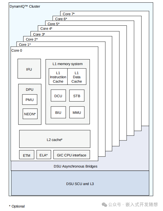 Functional OverviewThe system registers of this CPU primarily provide the following functions:
- System control and configuration
- Memory Management Unit (MMU) configuration and management
- Cache configuration and management
- System performance monitoring
- Generic Interrupt Controller (GIC) configuration and management.
Power ManagementPower management includes dynamic power management and static power management, where dynamic power management encompasses clock gating and Dynamic Voltage and Frequency Scaling (DVFS), while static power management includes dynamic retention and power-down.For clock gating, the ARMv8-A architecture provides the WFI (wait for interrupt) and WFE (wait for event) instructions, which can turn off the core’s clock while the core remains fully powered and all states are retained. WFI is typically used in idle CPU scenarios, suitable for situations requiring long waits for interrupts, such as idle threads, while WFE is appropriate for synchronization scenarios in multi-core systems, such as spin locks. When a core attempts to acquire a lock that is already held, it executes WFE to enter standby mode until the core holding the lock releases it and executes the SEV (send event) instruction to wake the waiting core.The diagram below shows the power domains of the A55 core, which include PDCPU<n>, PDADVSIMD<n>, and PDSYS.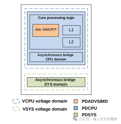 The diagram below illustrates the modes of the core’s power domain and their transitions.
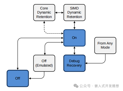 The power-down sequence for the A55 core consists of two parts, starting with the following software sequence:1. Save all architecture-related states;2. Disable the GIC distributor or route interrupts to other cores;3. Set the CPUPWRCTLR.CORE_PWRDN_EN bit to 1 to indicate a request to the power controller for the core to power down;4. Execute the Instruction Synchronization Barrier (ISB) instruction;5. Execute the WFI instruction.Then, the hardware operation occurs. After the core receives a power-down request from the power controller, the hardware will flush and turn off the L1 and L2 caches, and then remove the core from coherence management.Memory Management UnitThe main functions of the Memory Management Unit include:
- Controlling the hardware for translation table lookups to access the translation table in memory;
- Performing virtual to physical address translation;
- Providing fine-grained memory system control through virtual-physical address mapping and memory attributes.
Entries in the Translation Table can be cached by the Translation Lookaside Buffer (TLB).The table below shows the internal components of the MMU: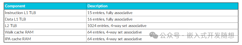 The L1 cache is divided into instruction and data parts, while L2 is a unified cache used to handle L1 cache misses. The L3 cache is part of the DynamicIQ Shared Unit (DSU) and does not have an independent TLB; the TLB functions related to address translation are mainly concentrated in L1 and L2, while the L3 cache primarily handles data caching and multi-core coherence maintenance. When the processor accesses memory, it first looks for address translation entries in the L1 TLB. If there is a miss in the L1 TLB, it will query the L2 TLB, and if there is also a miss in the L2 TLB, it will trigger a Page Table Walk to load new address translation entries into the TLB from memory.The L2 cache uses a set associative method, which is a compromise between direct-mapped and fully associative cache organizations. It combines the simplicity of direct mapping with the flexibility of full associativity, allowing for better utilization of cache space and reducing conflicts.The table below shows the types of device storage:
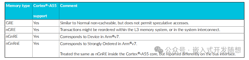 More InformationFor additional information, please refer to the official ARM documentation:https://developer.arm.com/documentation/100442/0200/?lang=enhttps://developer.arm.com/documentation/100453/0401/?lang=en