 Disclaimer: The article belongs to the author, and reproduction is for sharing and learning purposes only, not for any other commercial use! If there is any infringement, please contact us for deletion! (Mobile WeChat same number 15150147049)
The semiconductor manufacturing process can be divided into front-end processes and back-end processes. The front-end process mainly involves wafer manufacturing, while the back-end process mainly involves packaging and testing. Among them, packaging in the back-end process refers to a series of technical means to connect tested integrated circuit bare chips (Die) with external circuits, and to provide physical protection and environmental isolation through packaging materials, ultimately forming an independent electronic device that can be installed and operated.
Categories:
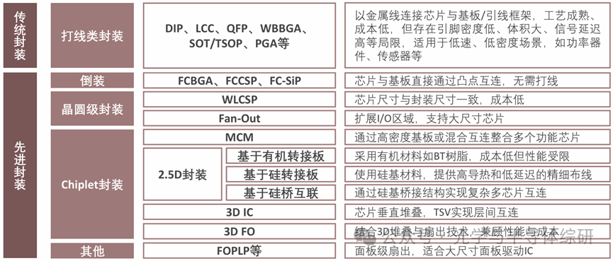
Advanced packaging differs significantly from traditional packaging processes. New applications in advanced packaging include wafer grinding and thinning, RDL (Redistribution Layer) fabrication, bump fabrication, TSV (Through-Silicon Via) fabrication, etc. The semiconductor packaging equipment required consists of existing back-end packaging equipment and newly added front-end equipment.
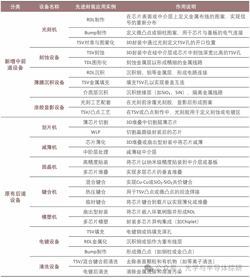
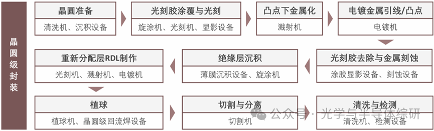
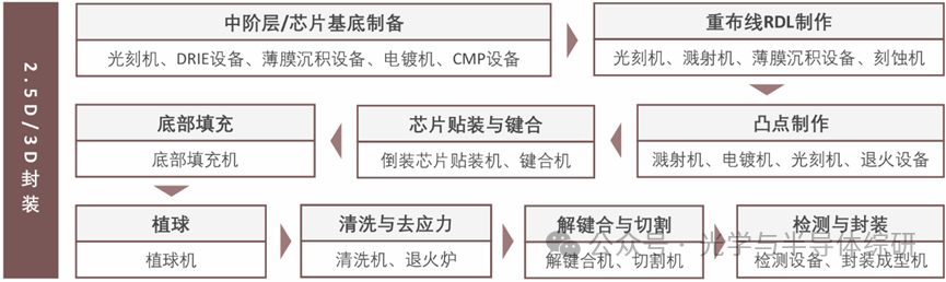
New front-end equipment for advanced packaging and existing back-end equipment
Technological upgrades of traditional back-end equipment under advanced packaging
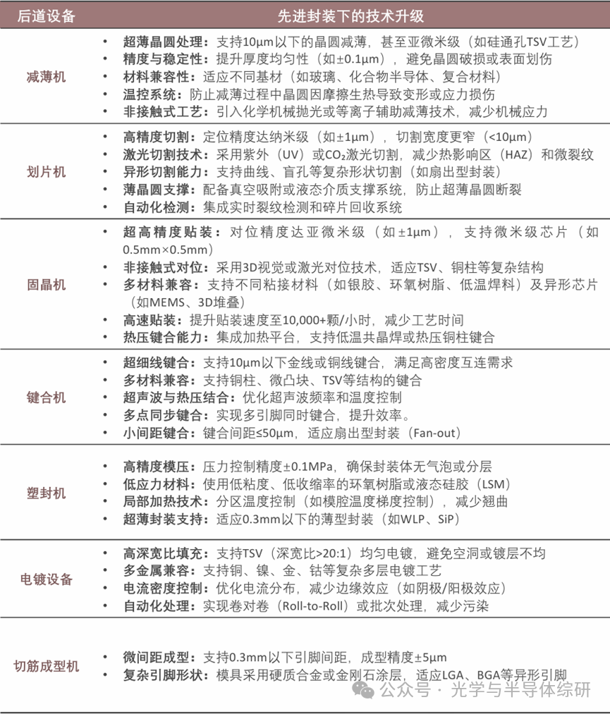
Thinning Machine
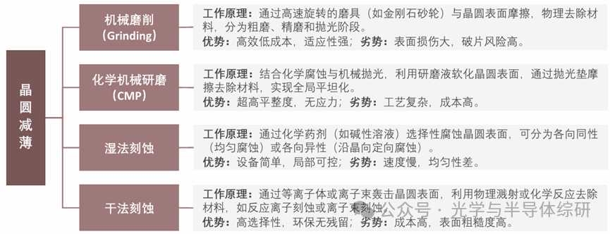
The wafer thinning machine (Wafer Thinning Machine) is a key piece of equipment in semiconductor manufacturing, primarily used for thinning semiconductor wafers to meet the requirements of subsequent processes (such as packaging and testing). Its core functions include reducing wafer thickness, improving surface quality, and adapting to advanced packaging. The wafer thinning process involves mechanically or chemically grinding the back of the wafer to reduce its thickness to a suitable level for packaging. The principle mainly involves methods such as mechanical grinding, chemical mechanical polishing, wet etching, and dry etching to remove material from the wafer surface. During the thinning process, strict control of the wafer’s flatness and thickness is required to ensure the quality and performance of the wafer. The wafer thinning machine is the key equipment for achieving the wafer thinning process.
A typical wafer thinning process usually includes several key steps: preparation, wafer fixation, rough grinding, fine grinding, polishing (optional), cleaning, inspection, and subsequent processing. The wafer thickness is generally about 750μm, and it can be thinned to around 100μm (the thickest wafers used for logic gates have a thickness of 100µm) to ensure mechanical stability and prevent warping during high-temperature processing. With the increasing application of 3D packaging, the requirement for wafer thickness to be reduced to 50-100μm or even below 50μm will significantly increase the quality demands for thinning equipment. Additionally, DRAM memory typically requires wafers with a thickness of 50μm, while MEMS memory usually has a thickness of about 30μm.

Sponsored Advertisement Display
Dicing Machine
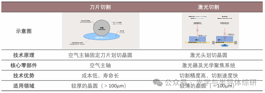
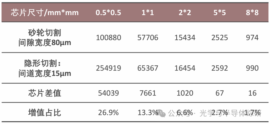
The wafer dicing machine is a device that uses blades or lasers to cut wafers containing many chips into individual chip particles. It is a key piece of equipment in the wafer cutting and WLP (Wafer Level Packaging) cutting stages of semiconductor back-end testing. The quality and efficiency of cutting directly affect the quality of the chips and production costs. Depending on the wafer process and product demand, a single wafer typically consists of hundreds to thousands of small chips, with most wafers having a gap of 40μm-100μm between the dice, known as the cutting lane. 99% of the chips on the wafer have independent functional modules (1% are edge dice, which do not have usable performance). To separate the small chips into individual dice, cutting processes are required. The dicing process mainly includes blade cutting and laser cutting, with laser cutting further divided into traditional laser cutting and laser stealth cutting. Traditional laser cutting requires a protective coating on the wafer surface, followed by applying high-energy laser to cut the silicon along the dicing lanes; stealth laser cutting, on the other hand, first uses laser energy to cut the interior of the wafer, then applies external pressure to the tape attached to the back to cause it to break, thus separating the chips.
In the context of advanced packaging, the application trend of laser cutting (especially laser stealth cutting) significantly surpasses traditional blade cutting, with core advantages including: 1) meeting the demand for high precision and low damage, protecting micro-nano structures in advanced packaging; 2) flexibly adapting to complex designs, such as thin wafers, heterogeneous integration, and 3D stacking.
Die Bonder (Die Attach Machine)

The die bonder (Die Attach Machine) is used to pick up chips from the already cut wafers and place them on the corresponding die flags on the substrate, using silver glue (Epoxy) to bond the chip and substrate together. Die bonders can place components at high speed and high precision, achieving key steps such as positioning, alignment, flip-chip, and continuous placement. Packaging die bonders are divided into FC (Flip Chip) die bonders, FO (Fan-Out) die bonders, and 2.5D/3D die bonders. According to application types, they can be classified into IC die bonders, discrete device die bonders, LED die bonders (die attach and COB die bonders), mainly used in the packaging processes of semiconductor chips, optical chips, optical modules, silicon photonic devices, sensors, etc.
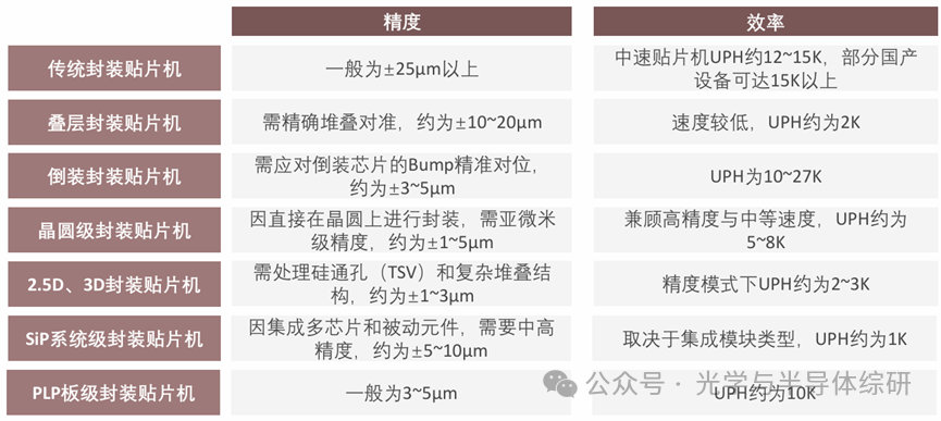
Due to advanced packaging technologies such as 3D stacking, system-in-package (SiP), and fan-out wafer-level packaging (FOWLP) requiring the handling of smaller components, denser layouts, and more complex structures, there are higher demands for the precision and efficiency of die bonders. In terms of precision, the current domestic IC die bonders generally have a precision of ±25μm or more, while the international leading level is ±3~5μm, with high-end models reaching ±1μm (such as ASMPT COS die bonders). Under advanced packaging demands, 3D NAND and HBM require precision of ±1~3μm to ensure accurate alignment and increased interconnection density between chips and substrates; in terms of efficiency, the current domestic equipment has a UPH (Units Per Hour) of about 12-15K, while international leading models of mid-high precision equipment can reach UPH of 15-20K, and high-speed models (such as ASMPT FC/FB series) can exceed 25K. In advanced packaging production lines, to meet high capacity demands, UPH needs to be increased to over 20K, even 30K.
Bonding Machine
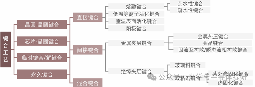
Bonding refers to the process of attaching two smooth and clean wafers together using physical or chemical methods to assist semiconductor manufacturing processes or to form heterogeneous composite wafers with specific functions. There are various types of bonding technologies, classified into wafer-to-wafer bonding (W2W) and die-to-wafer bonding (D2W) based on wafer types; temporary bonding and permanent bonding based on whether debonding is required after bonding; and direct bonding, indirect bonding, and hybrid bonding based on whether auxiliary interface layers are introduced. Additionally, traditional bonding methods such as wire bonding are gradually being replaced by advanced methods such as flip-chip bonding and hybrid bonding.
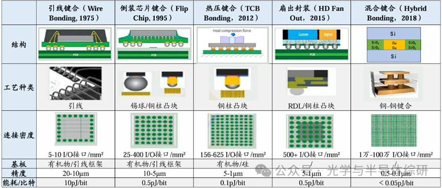
With the continuous advancement of packaging technology, bonding equipment now needs to achieve higher precision and finer energy control. According to Besi’s data, with the promotion of the latest hybrid bonding technology, bonding precision has significantly improved from the original 5-10/mm² to 10K-1MM/mm², while energy consumption has been significantly reduced to only 0.05pJ per bit. Entering the post-Moore era, the focus of packaging technology has shifted to improving transmission efficiency and reducing chip size. Traditional wire bonding technology completes electrical connections using metal wires, but due to physical space limitations and signal delay issues, it is difficult to meet the demands of modern advanced packaging. To overcome these challenges, thermocompression bonding (TCP) and hybrid bonding are seen as key technological development directions. In particular, hybrid bonding technology replaces traditional wires with copper contacts, achieving direct electrical interconnection between wafers, increasing interconnection density by more than ten times compared to the past. However, this method places extremely high demands on the smoothness, cleanliness, and alignment accuracy of the wafer surfaces. Currently, hybrid bonding technology is mainly applied in high-performance storage fields, such as HBM and 3D NAND.
Plastic Packaging Machine
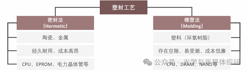
The plastic packaging machine is a device that encapsulates chips in plastic (such as epoxy resin) or other materials, with its core function being to provide physical protection and electrical insulation for the chips, firmly bonding the chip, lead frame, or substrate with the package, ensuring signal transmission and heat dissipation performance. The plastic packaging process typically includes the following steps: chip mounting, preheating and mold closing, injection molding/pressure molding, curing, trimming, and forming.
The plastic packaging process can generally be divided into hermetic sealing and molding methods:
Hermetic sealing refers to sealing with ceramic plates or metal covers; molding refers to melting and then curing plastic epoxy materials for sealing. Among these two methods, hermetic sealing is rarely used currently, while molding using epoxy resin is more commonly adopted.
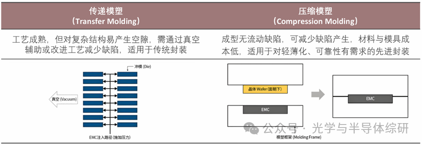
Molding can be further divided into transfer molding and compression molding: transfer molding pushes melted epoxy resin through narrow channels in the mold under pressure, injecting it into the mold cavity, and curing it into shape. The transfer molding process is mature but can easily produce voids in complex structures (such as multi-layer chips), requiring vacuum assistance or improved processes to reduce defects, making it suitable for traditional packaging; compression molding directly places epoxy resin particles into the mold, heating and melting them, then applying high pressure to evenly fill the mold and cure. Compression molding has advantages such as defect detection, low cost, and minimal environmental impact, making it particularly suitable for advanced packaging scenarios that require lightweight and high reliability (such as WLCSP and multi-layer packaging).
Source:Optics and Semiconductor Research
Disclaimer: The article belongs to the author, and reproduction is for sharing and learning purposes only, not for any other commercial use! If there is any infringement, please contact us for deletion! (Mobile WeChat same number15150147049)

WeChat number 15150147049 (please note company name + name)