
This article explains NVIDIA’s latest hardware chip, Orin, which is commercially used in intelligent driving.
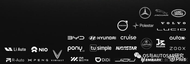
Currently, Orin orders are booming, with major companies such as SAIC’s R and Zhiji, Li Auto L9, NIO ET7, XPeng’s new generation P7, BYD, Volvo XC90, and autonomous truck company Zhijia Technology, as well as star enterprises like Cruise, Zoox, Didi, Pony.ai, AutoX, and software company Momonta, all using the Orin platform for development. The lineup is impressive, making it the strongest computing chip on the planet.
1. NVIDIA Smart Driving SoC Chip Development History
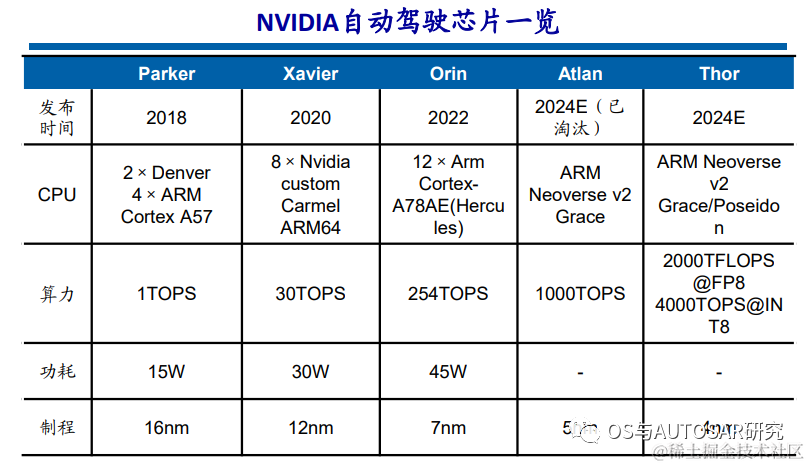
Since 2015, NVIDIA has entered the vehicle SoC and vehicle computing platform field to provide basic computing power for autonomous driving. Since then, NVIDIA has released a vehicle-grade SoC chip almost every two years, continuously increasing computing power levels. In 2020, the Xavier chip had a computing power of 30 TOPS, while the Orin released in 2022 has a computing power of 254 TOPS. At the 2022 autumn GTC conference, a new autonomous driving chip, Thor, was announced, with a computing power of 2000 TFLOPS@FP8 and 4000 TOPS@INT8, replacing the previously released Altan, which had a computing power of 1000 TOPS.
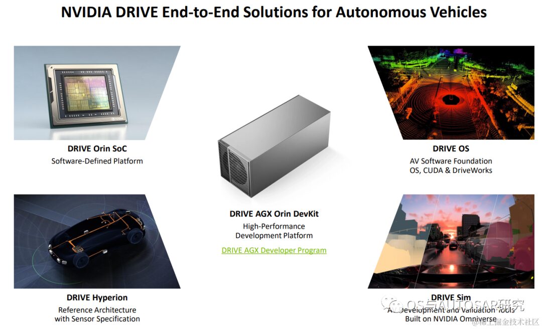
In other words, the latest commercially available chip is Orin. The lineup of car manufacturers using NVIDIA is powerful, as shown in the figure below:
1.1 Xavier Platform
NVIDIA launched the Xavier platform at CES 2018 as an evolution of the Driver PX2. NVIDIA claims that Xavier is “the world’s most powerful SoC (System on Chip)”. Xavier can process autonomous driving perception data from vehicle radar, cameras, lidar, and ultrasound sensors with higher efficiency than similar products on the market and a smaller size. “NVIDIA® Jetson AGX Xavier™ sets a new benchmark for computing density, energy efficiency, and AI inference capability for edge devices.”
The XPeng P7, launched in April 2020, became the first mass-produced model equipped with the NVIDIA DRIVE AGX Xavier autonomous driving platform. The P7 is equipped with 13 cameras, 5 millimeter-wave radars, and 12 ultrasonic radars, integrated with the open NVIDIA DRIVE OS operating system.
The Xavier SoC is based on TSMC’s 12nm FinFET process, integrating 9 billion transistors, with a chip area of 350 square millimeters. The CPU uses NVIDIA’s self-developed 8-core ARM64 architecture (code-named Carmel), integrated with a Volta architecture GPU (512 CUDA cores), supporting FP32/FP16/INT8. At 20W power consumption, single-precision floating-point performance is 1.3 TFLOPS, and Tensor core performance is 20 TOPS, reaching 30 TOPS when unlocked to 30W.
Xavier is a highly heterogeneous SoC processor, integrating up to eight different processor cores or hardware acceleration units. This allows it to simultaneously and in real-time process dozens of algorithms for tasks such as sensor processing, ranging, positioning and mapping, vision and perception, and path planning.
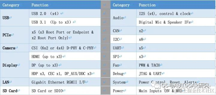
In addition to powerful computing resources, the Xavier SoC has a rich set of I/O interface resources:
The main processor of Xavier can meet the ASIL-B functional safety level requirements. Ecotron has built a high-performance central computing platform for L3/L4 autonomous driving, based on NVIDIA’s Xavier SoC and Infineon TC297 MCU. According to the design scheme, the Xavier smart processor is used for environmental perception, image fusion, path planning, etc., while the TC297 MCU is used to meet ISO26262 functional safety requirements (ASIL-C/D level) for control application scenarios (i.e., as Safety Core), such as safety monitoring, redundant control, gateway communication, and vehicle control.

Structure diagram of the dual Xavier + TC297 MCU scheme:
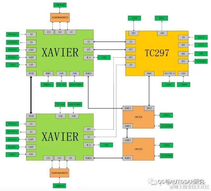
This usage is from the old platform, but its scheme has been continuously inherited, i.e., the TCXXX vehicle control chip operates independently of AUTOSAR. Here, two domains are illustrated: Smart Driving Domain (NVIDIA) + Vehicle Control Domain (TC), while the cockpit generally uses mature and inexpensive mobile Android technology. It remains to be seen whether there is a possibility of achieving a centralized architecture in the future; currently, it is still a three-domain architecture.
1.2 Orin Platform

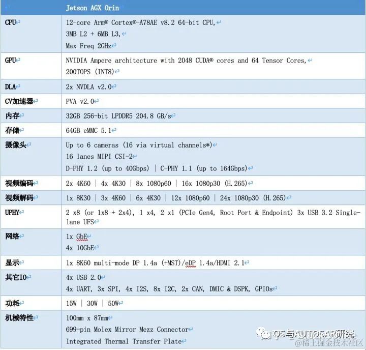
In December 2019, NVIDIA released the next generation Orin chip and computing platform aimed at autonomous driving and robotics. It features ARM Hercules CPU cores and NVIDIA’s next-generation GPU architecture. The Orin SoC contains 17 billion transistors, nearly double the number of transistors in the Xavier SoC, with 12 ARM Hercules cores, integrating NVIDIA’s next-generation Ampere architecture GPU, providing 200 TOPS@INT8 performance, nearly 7 times that of the Xavier SoC. The Orin SOC samples were available in 2021, and mass production for automakers began in 2022.
In May 2020, at GTC, NVIDIA introduced the upcoming new generation autonomous driving Drive AGX Orin platform, which can carry two Orin SoCs and two NVIDIA Ampere GPUs, achieving a comprehensive performance improvement from entry-level ADAS solutions to L5 autonomous taxi (Robotaxi) systems, with a maximum computing power of 2000 TOPS. Future L4/L5 autonomous driving systems will require more complex and powerful autonomous driving software frameworks and algorithms. With strong computing performance, the Orin computing platform will help run multiple autonomous driving applications and deep neural network model algorithms concurrently.
As a vehicle intelligent computing platform designed specifically for autonomous driving, Orin can reach ISO 26262 ASIL-D level functional safety standards.
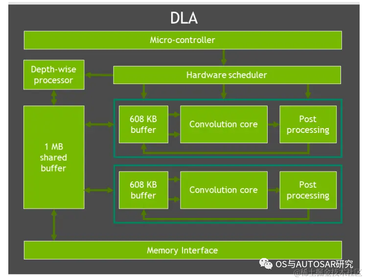
With advanced 7nm process technology, Orin has excellent power consumption levels. With a massive computing power of 200 TOPS, the TDP is only 50W. NVIDIA Orin processor functional module diagram
The following table shows the performance parameters of the Jetson AGX Orin SoC:
1.3 Thor Platform
NVIDIA DRIVE Thor is NVIDIA’s next-generation centralized vehicle computing platform that can run advanced driver assistance applications and in-vehicle infotainment applications on a single safe and reliable system. The DRIVE Thor super chip, with our new CPU and GPU breakthroughs, can provide outstanding performance of 20 trillion floating-point operations while reducing overall system costs, with mass production planned to start in 2025.
It can be seen that the three domains are starting to become two domains, with smart driving and cockpit unifying, and the unification of domains seems to be just around the corner, requiring only the last vehicle control MCU to be resolved with safety technology.
DRIVE Thor has also made incredible leaps in deep neural network accuracy. The Transformer engine is a new component of NVIDIA’s GPU Tensor Core. The transformer network processes video data as a single perception frame, allowing the computing platform to process more data over time.
This SoC can perform multi-domain computing, meaning it can partition tasks between autonomous driving and in-vehicle infotainment. This multi-computing domain isolation allows concurrent time-critical processes to run uninterrupted. On a single computer, the vehicle can simultaneously run Linux, QNX, and Android. Typically, these types of functions are controlled by dozens of electronic control units distributed throughout the vehicle. Manufacturers can now leverage DRIVE Thor’s ability to isolate specific tasks to integrate vehicle functions rather than relying on these distributed ECUs.
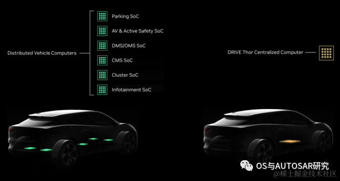
All vehicle displays, sensors, etc., can connect to this single SoC, simplifying the extremely complex supply chain for automotive manufacturers.
Reference: https://blogs.nvidia.com/blog/drive-thor/
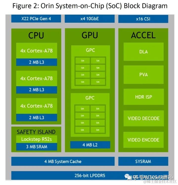
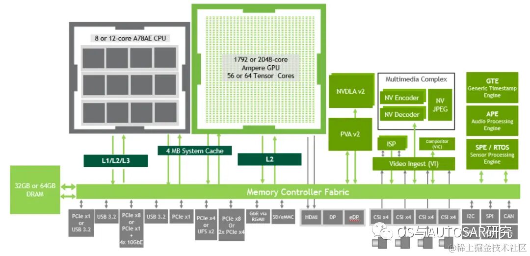
2. Introduction to Orin Architecture
Taking Orin-x as an example, the CPU includes a main CPU complex based on Arm Cortex-A78AE, providing general high-speed computing capabilities; and a functional safety island (FSI) based on Arm Cortex-R52, which provides isolated on-chip computing resources, reducing the need for external ASIL D functional safety CPU processing.
The GPU is NVIDIA® Ampere GPU, providing advanced parallel processing computing capabilities for CUDA language and supporting various tools such as TensorRT, a deep learning inference optimizer and runtime that provides low latency and high throughput. Ampere also offers state-of-the-art graphics capabilities, including real-time ray tracing. Domain-specific hardware accelerators (DSA) are a set of dedicated hardware engines designed to offload various computational tasks from the computing engine and execute these tasks with high throughput and high energy efficiency.
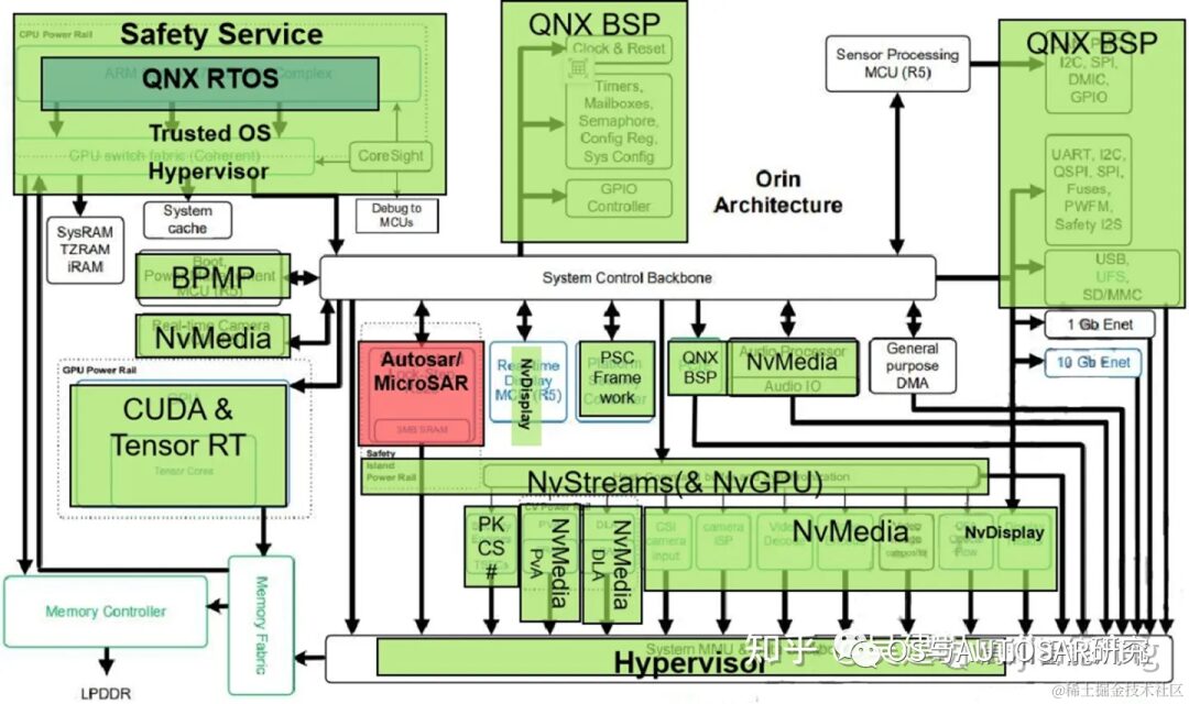
The overall chip internal architecture design is mainly functionally designed by partitioning. This includes the underlying operating system software QNX BSP (clock source & system reboot, CAN/SPI/I2C/GPIO/UART controllers, configuration registers, system configuration), real-time operating system QNX RTOS, NVIDIA multimedia processing module (sensor processing module MCU (R5), PVA, DLA, Audio Processor, MCU R5 configuration for real-time camera input), classic Autosar processing module (for Safety Island Lock-Step R52s), safety service (ARM Cortex-A78AE CPU Complex, CPU Switch fabric Coherent, information security PSC), and neural network processing module (CUDA & TensorRT).
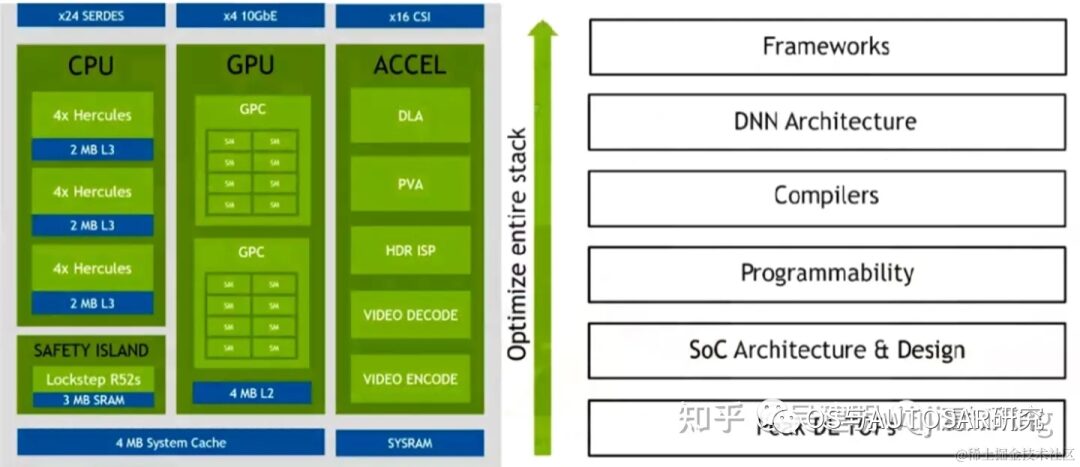
The following diagram shows the high-level architecture of the SoC, divided into three main processing complexes: CPU, GPU, and hardware accelerators.
2.1 CPU Related

In the Orin system architecture, the CPU returns from the previously self-developed Carmel architecture to the ARM Cortex-A78 based on 5nm process technology. The CPU in Orin-x includes 12 Cortex-A78 cores, providing general high-speed computing compatibility. At the same time, the Arm Cortex R52 is based on functional safety design (FSI), providing independent on-chip computing resources, eliminating the need for additional CPU (ASIL D) chips to provide functional safety levels.
The CPU family supports features including debug debugging, power management, Arm CoreLink interrupt controller, and error detection and reporting. The CPU needs to monitor the overall performance of the chip, and the performance monitoring unit in each core provides six computing units, each capable of calculating any event in the processor. Based on the PMUv3 architecture, these computing units will collect different statistics during each runtime and operate on the processor and storage system.
2.2 GPU
NVIDIA Ampere GPU provides an advanced parallel processing computing architecture. Developers can use CUDA language for development (detailed explanations of the CUDA architecture will follow) and support various tools from NVIDIA (such as APIs for developing Tensor Core and RT Core applications). A deep learning interface optimizer and a real-time operating system can deliver low latency and efficient output. The Ampere GPU can also provide several features to achieve high-resolution and high-complexity image processing capabilities (such as real-time optical flow tracking).
-
Sparsification:Fine-grained structured sparsity doubles throughput and reduces memory consumption. Floating-point processing capability: Achieves 2 times CUDA floating-point performance per clock cycle.
-
Cache:The streaming processor architecture can increase L1 cache bandwidth and shared memory, reducing cache miss latency. Enhancing asynchronous computing capabilities, with L2 cache compression.
2.3 Accelerator
Domain-specific hardware accelerators (DSAs, DLA, PVA) are a set of special-purpose hardware engines that realize multitasking, high efficiency, and low power characteristics of the computing engine. The computer vision and deep learning cluster includes two main engines: programmable vision accelerator PVA and deep learning accelerator DLA (the DLA processor has been removed in the latest mid-range computing Orin n chip).
PVA is the second-generation NVIDIA visual DSP architecture, a special application instruction vector processor designed specifically for computer vision, ADAS, ADS, and virtual reality systems. PVA has several key elements that adapt well to prediction algorithm domains, with low power consumption and latency. Orin-x requires internal R cores (Cortex-R5) subsystems for PVA control and task monitoring. A PVA cluster can perform the following tasks: a bidirectional vector processing unit (VPU) with vector cores, instruction cache, and 3 vector data storage units. Each unit has 7 visible slots, containing both scalar and vector instructions. Additionally, each VPU has a storage capacity of 384 KBytes.
DLA is a fixed-function engine used to accelerate inference operations in convolutional neural networks. Orin-x has a dedicated DLA to implement the second-generation NVIDIA DLA architecture. DLA supports accelerating convolution, deconvolution, activation, pooling, local normalization, and fully connected layers of CNN layers. Ultimately supporting optimized structured sparsity, deep convolution, and a dedicated hardware scheduler to maximize efficiency.
2.4 Second-Generation Vision Accelerator PVA and VIC
Orin also includes a Gen 4.2 video imaging compositor (Video Imaging Compositor, VIC) 2D engine, supporting image processing functions such as lens distortion correction and enhancement, temporal denoising, video clarity enhancement, pixel processing (color space conversion, scaling, blending, and compositing).
To call multiple hardware components (PVA, VIC, CPU, GPU, ENC, etc.) on the Orin SoC, NVIDIA developed the Vision Programming Interface (VPI). As a software library, VPI includes various image processing algorithms (such as frame filtering, convolution, image rescaling, and remapping) and computer vision algorithms (such as Harris corner detection, KLT feature tracking, optical flow, background subtraction, etc.).
2.5 Memory and Communication
The above diagram shows how various components of Orin communicate and interact through the memory controller structure (Fabric) and DRAM.
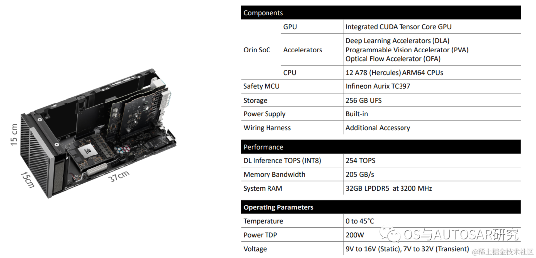
Orin supports a maximum of 64GB of 256-bit LPDDR5 and 64GB of eMMC. DRAM supports a maximum clock speed of 3200MHz, with each pin at 6400Gbps, supporting a memory bandwidth of 204.8GB/s, which is 1.4 times the memory bandwidth of Xavier and 2 times the storage.
3. Orin-Based Autonomous Driving Platform Architecture Design
Conventional SOC system architecture typically includes a conventional SOC + MCU dual-chip or even triple-chip design. Due to the advantages of computing performance, SOC is generally better than MCU in front-end perception and planning computing application scenarios.
MCUs have high functional safety levels and can serve as verification outputs for control execution. The industry has been divided on whether NVIDIA chips can independently undertake tasks like TDA4 as ultra-heterogeneous chips. In principle, both the Xavier and Orin series are designed to possess rich AI and CPU computing capabilities. Considering the development of autonomous driving systems above L2+, this capability can fully adapt to the overall solution design. However, for safety-critical vehicle control MCUs, it is not just about advanced technology; it mainly relates to installed quantities, and it must be safe to use.
3.1 Safety Considerations

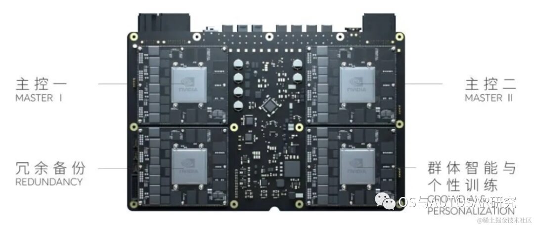
It can be seen that the basic R52 core achieves ASIL-D, while others generally only meet ISO 26262. Therefore, a Safety MCU (SMCU) is needed as an auxiliary to implement the vehicle control domain. For example, Infineon’s Aurix TC series and Renesas’ RH850 series can serve as MCUs to interface with Orin’s SMCU. This SMCU can serve as the power control and serious failure fault avoidance for the entire system development. The SMCU TC397 can be seen in NVIDIA’s sold development platform, as shown in the figure below:
Through trusted security loading technology, ATF stores BL1 in ROM, which has a security check for BL2, forming a chain of secure loading. All low-level boot steps, including u-boot, can be ensured to be secure via signed binary files. Their keys can be stored in one-time programmable fuses within the CPU. U-boot itself can be configured to use signed FIT images, providing a secure boot chain all the way to the Linux kernel. The initial ROM bootloader and TegraBoot also support fully redundant boot paths.
3.2 FSI Introduction
The above diagram shows how to load FSI and the underlying related module drivers in NVIDIA series chips. In terms of functional safety design, the Orin series achieves ASIL D system capability design and ASIL B/D random error management capability design. This includes breaking down ASIL requirements based on the SOC chip hardware to each core, ensuring that inter-core design consistency meets ASIL D requirements, and applying standard ASIL D development processes to the entire functional safety design, addressing safety design across various aspects such as safety processes, Drive AGX, operating system Drive OS, Drive Work, sensors, redundant architecture design, and safety policies.
The functional safety island (FSI) of NVIDIA series chips consists of a cluster of Cortex-R52 and Cortex-R5F real processors, with a dedicated I/O controller for time-sensitive processing. For instance, the FSI module in Orin-X has its own voltage rail, oscillator, PLL, and SRAM to minimize interactions with other modules within the SOC and ensure interference-free operation between the above modules.
The Cortex-R52 processor, also known as the safety CPU, has 4 cores in dual-core lock-step mode (a total of 8 physical cores), capable of running classic AUTOSAR operating systems, error handling, system fault handling, and other customer workloads, with comprehensive performance around 10K DMIPs.
The Cortex-R5F processor, also known as the cryptographic hardware security module (CHSM), is used for cryptographic and security use cases via CAN interface, such as secure vehicle communication (SecOC).
The overall FSI mechanism includes the following safety instructions and control interface information:
1. Secure and CHSM CPU tightly coupled memory, instructions, and data cache for each core.
2. A total of 5MB of dedicated on-chip RAM on the safety island to ensure code execution and data storage can remain within the FSI.
3. The island has dedicated I/O interfaces for communication with external components, including 1 UART and 4 GPIO ports.
4. Hardware safety mechanisms, such as DLS, CRC, ECC, parity, and timeout for all IPs within the FSI. Dedicated thermal, voltage, and frequency monitors.
5. Logical isolation to ensure enough error recovery time from the rest of the SOC.
3.3 TESC
Tegra is a unique information security chip kernel in NVIDIA chips. The Tegra Security Controller (TESC) is an information security subsystem with its own trusted root ROM, IMEM, DMEM, Crypto accelerators (AES, SHA, RNG, PKA), key link, and key storage. TESC provides an on-chip TEE (Trusted Execution Environment) that can run NVIDIA-labeled processing code. TESC is a typical secure video playback solution, downloading the information security runtime required HDCP1.x and 2.x connection authorization and complete line-end connection detection.
1) HDCP 1.4 on line-end HDMI 1.4 and HDCP 2.0 2.1 on line-end HDMI 2.3; HDCP connection management does not expose protected content and does not require software keys running on the CPU. Two software-programmable independent instruction queues for HDCP link management (up to 16 instructions); the entire chip can independently disable HDMI output upon HDCP status check failure.
2) Platform security controller; it is a high-security subsystem that can protect and manage assets (keys, fuses, functions, features) within the SOC and provide trusted services, enhancing resistance to attacks on the SOC and increasing protection levels against software and hardware attacks on the subsystem itself.
3) Key management and protection; PSC will be the only mechanism to access the most critical keys in the chip. This subsystem represents the highest level of protection in Orin-x, and it is highly resilient to various software and hardware attacks.
4) Trusted services; for example, during SOC secure boot, the main PSC service can complete effective secure authentication, provide additional keys/IDs/data, key access and management, random number generation, and trusted time reporting.
5) Information security monitoring. PSC will be responsible for regular security management tasks, including continuous assessment of the SOC’s security status, proactive monitoring of known or potential attack patterns (e.g., voltage faults or thermal attacks), reducing the risk of hardware attacks, and taking effective measures upon detecting attacks. PSC will be able to accept various software updates as solutions to enhance the robustness of the on-site system.
3.4 Security Engine (SE)
NVIDIA’s security engine SE supports all information security assurance capabilities, including:
NIST-compliant symmetric and asymmetric encryption and hash algorithms, side-channel countermeasures (AES/RSA/ECC), independent parallel channels, hardware key access control (KAC) (based on rules, enhancing hardware access control for symmetric keys), 16x AES, 4x RSA/ECC keyholes, hardware key isolation (only for AES keyholes), read protection (only for AES keyholes), hardware keyhole functions, key wrapping/unwrapping features (AES->AES keyholes), key separation from keyholes (KDF->AES keyholes), random key generation (RNG->AES keyholes).
4. GPU Programming CUDA
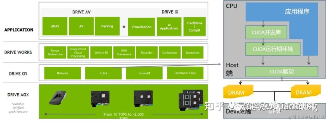
The above image illustrates the CUDA architecture diagram, depicting the relationship between the CPU, GPU, applications, CUDA development libraries, runtime environment, and drivers.
4.1 GPU Software Architecture
The AI algorithms used in the autonomous driving field are mostly parallel structures. Deep learning for image recognition, machine learning for decision-making and reasoning, and supercomputing all require massive parallel computing, making them more suitable for GPU architecture. The number of layers in a neural network (the more hidden layers, the more precise the neural network’s simulation results) significantly affects its predictive results. GPUs, adept at parallel processing, can effectively process and optimize neural network algorithms. Since each computation in a neural network is independent of others, any computation does not rely on the results of others, allowing all these independent computations to be performed in parallel on the GPU. Typically, a single convolution computation performed on a GPU is slower than on a CPU, but for the overall task, the CPU processes in a serial manner, needing to complete each step sequentially, thus its speed is significantly slower than that of a GPU. Therefore, convolution operations can be accelerated using parallel programming methods and GPUs.
NVIDIA forms a product matrix through CPU + GPU + DPU, fully tapping into the data center market. Leveraging the innate advantages of GPUs in AI, NVIDIA has entered the data center market. To address various issues such as internal chip bandwidth and system-level interconnects, NVIDIA has introduced the Bluefield DPU and Grace CPU, enhancing overall hardware performance.
For NVIDIA’s GPU, a GPC contains one raster engine (ROP) and 4 texture processing clusters (TPCs), with each engine able to access all storage.
4.2 CUDA Programming
CUDA (Compute Unified Device Architecture) serves as a central node connecting AI, and the CUDA + GPU system has significantly propelled the development of AI. Workstations, servers, and clouds equipped with NVIDIA GPU hardware provide the necessary software toolchain for training (Train) and inference (Inference) required for AI computing in autonomous driving systems through the CUDA software system and developed CUDA-XAI library, serving numerous frameworks and cloud services, making it an indispensable part of the entire NVIDIA chip software development.
CUDA is a special computing system/algorithm customized for NVIDIA GPU platforms, generally only usable on NVIDIA’s GPU systems. From the developer’s perspective, we will discuss how to develop at different software levels on the CUDA architecture in NVIDIA’s Orin series chips.
In terms of the composition of the CUDA architecture, it consists of three parts: development libraries, runtime environment, and drivers.
-
“Developer Lib development library” is an application development library provided based on CUDA technology. For example, highly optimized general mathematical libraries, i.e., cuBLAS, cuSolver, and cuFFT. Core libraries, such as Thrust and libcu++; communication libraries, such as NCCL and NVSHMEM, and other packages and frameworks that can be built upon.
-
“Runtime environment” provides application development interfaces and runtime components, including definitions of basic data types and functions for various computations, type conversions, memory management, device access, and execution scheduling.
-
“Driver part” is the device abstraction layer that enables CUDA on GPUs, providing abstract access interfaces for hardware devices. The runtime environment provided by CUDA is also implemented through this layer for various functions.
Under the CUDA architecture, a program is divided into two parts: the host side and the device side. The host side refers to the part executed on the CPU, while the device side is executed on the display chip (GPU). The device-side program is also called a