Previous Articles:
-
Introduction to ARM Processors 1 – Overview
Introduction
This article is the second part of the introduction series on ARM processors, mainly introducing some basic technologies and concepts of modern superscalar out-of-order processors. We will take the Cortex-A9 processor as an example to see which technologies are used to enhance performance, laying the foundation for our subsequent understanding of the microarchitecture of ARM processors and comparative analysis.
Note: In fact, explaining the key points of modern processor technology can be quite complicated. Each technology might require an article, and since I am not from a related professional background, my energy and understanding depth are limited. Therefore, I can only roughly list some basic concepts. For more in-depth analysis, you can refer to the articles listed in this article.
Some Features of Modern Processors
We mainly understand the following main features of modern processors:
-
Multi-Core -
Pipeline -
Superscalar -
Out Of Order Execution -
Branch Prediction -
Cache and MMU
Multi-Core
When a single CPU’s clock frequency exceeds a certain level, the cost and heat dissipation of the CPU become significant issues. If we want to further enhance processor performance, a natural idea is to adopt a strategy similar to a human wave tactic, increasing multiple cores in one CPU, allowing multiple CPUs to execute concurrently. Previously, one person was working, and now seven or eight people are working together, which naturally increases efficiency. However, due to the correlation between processes distributed across various CPUs, IPC (Inter-Process Communication) may sometimes be needed, requiring synchronization operations to ensure certain timing, and the existence of critical sections also requires mutual exclusion. Therefore, the increase in the number of CPU cores does not necessarily lead to a proportional increase in performance, especially in embedded devices, where chip area and power consumption constraints must also be considered. We cannot indefinitely improve performance just by stacking CPU cores.
Pipeline
Looking at the execution process of the CPU, it can be divided into: IF (Instruction Fetch), ID (Instruction Decode), EX (Execution), MEM (Memory Access), and WB (Register Write Back). Modern processors typically break down the CPU execution steps even further, but here we use these classic five steps to illustrate the concept of pipelining.
Just like a factory producing a product, when the manufacturing process is divided into steps, each step can operate efficiently at full load, greatly enhancing efficiency. The CPU execution process is similar. As shown below, ideally, from the fifth cycle onwards, all functional units can execute concurrently without interruption. In reality, aside from delays between components, some hazards can arise, leading to pipeline stalls, which we will introduce later.
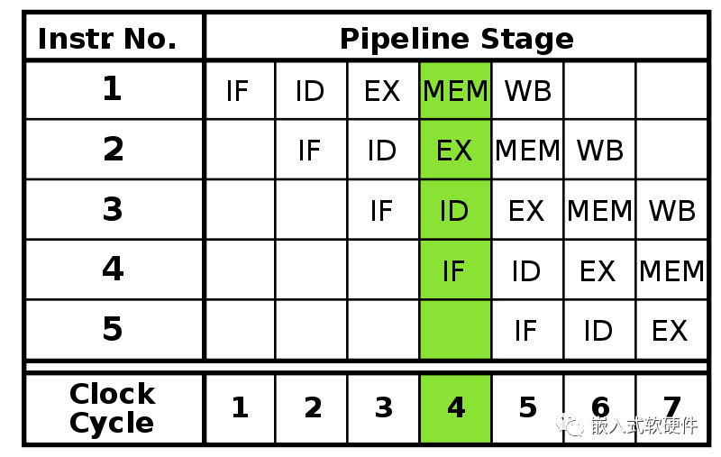
Without considering other factors, the clock frequency is limited by the longest and slowest stage in the pipeline. If the pipeline stages (especially the time-consuming stages) are broken down into simpler sub-stages, then the entire processor’s main frequency can run higher! Thus, pipelines with more finely divided stages are referred to as Super Pipelining. However, having too many pipeline stages is not necessarily better; nowadays, it generally does not exceed 15 stages.
Superscalar
Superscalar
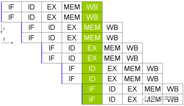
Each functional unit in a pipeline can only process one instruction at a time. With multiple issue capabilities, each functional unit can handle multiple instructions simultaneously. This is similar to each worker on a factory assembly line being highly capable, able to finish their own task while also having some spare capacity. To maximize the efficiency of each worker on the assembly line, an additional assembly line can be added. As shown in the diagram, each execution unit can handle two instructions. The term ‘multiple issue’ refers to the CPU’s execution units having multiple ports, allowing multiple instructions to be issued to different execution units in the same clock cycle, typically occurring after instruction decoding.
Hazards in Pipelining
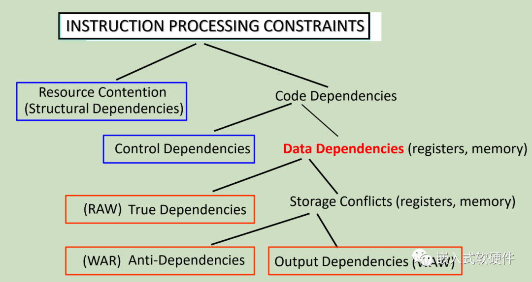
Of course, there are some hazards (also some dependencies) that need to be resolved in pipelining to achieve true performance enhancement. Let’s first look at the general types of hazards:
-
Structural hazards, also known as resource contention, refer to competition for hardware resources; -
Data hazards, which can be subdivided into RAW, WAR, and WAW types, will be elaborated later; -
Control hazards mainly occur during branch jumps.
Structural Hazards
Essentially, this is a resource contention issue at the hardware level. The CPU may be running two different instructions at different stages in the same clock cycle. However, these two different stages may use the same hardware circuitry. For example, a Harvard architecture processor has two sets of hardware to simultaneously complete data and instruction memory accesses, which can improve performance compared to the von Neumann architecture, which shares a single set of data and instruction paths.
Data Hazards
Data hazards occur when multiple instructions being executed simultaneously have data dependencies. These data dependencies can be categorized into three main types: Read After Write (RAW), Write After Read (WAR), and Write After Write (WAW).
-
RAW (Read After Write): For example, in the following instruction sequence, if the second instruction reads x5 before the first instruction writes to x5, it will cause a logical error. This is a data dependency (also known as True Dependency).
add x5, x4, x6 add x4, x5, x2 -
WAW (Write After Write): For example, in the following instruction sequence, if the second instruction writes to x5 before the first instruction writes to x5, it will cause a logical error. This is an output dependency.
add x5, x4, x6 add x5, x3, x2 -
WAR (Write After Read): Also known as read-before-write dependency. For example, in the following instruction sequence, the first instruction will read x4, and the second instruction will write to x4. In pipelining, if the second instruction writes to x4 before the first instruction reads x4, the first instruction will read an incorrect value. This is an anti-dependency.
add x5, x4, x6
add x4, x3, x2
Control Hazards
If there are conditional branches like if…else or for/while loops, the program will jump, affecting subsequent instruction fetching and decoding, leading to control hazards.
Branch Prediction
If control hazards occur without taking other measures, the processor will wait for the branch instruction to pass through the execution stages of the pipeline before sending the next instruction into the pipeline, which can cause pipeline stalls or the penalty of clearing all subsequent pipelines. Branch prediction can alleviate this type of problem to some extent, but if the prediction fails, there will still be such penalties.
Types of Branch Jumps
There are mainly two types of branch jumps: conditional and unconditional, direct and indirect jumps, as shown in the following table:
| Conditional | Unconditional | |
|---|---|---|
| Direct | if else and other conditional statements, for loop statements | call statements (function calls), goto statements |
| Indirect | return statements (function returns), virtual function/function pointer calls |
The target addresses of branches are generally divided into two types:
-
Direct jumps (PC-relative, direct): The offset is fixed in the instruction as an immediate number, so the target address is also fixed. -
Indirect jumps (absolute, indirect): The target address comes from a general-purpose register, and the value of the register is not fixed.
Among them, Unconditional and Call are considered direct jumps; conditional jumps (the branch value changes based on variable values, having multiple paths and directions), as well as Return in unconditional jumps (which has multiple callers), are all register-related.
Static Prediction
The simplest static branch prediction method is to randomly choose one branch: 1) Assume the branch will definitely be taken; 2) Assume the branch will definitely not be taken; this gives an average hit rate of 50%. A more accurate method is to use prior execution results for statistical analysis to try to predict whether the branch will jump.
Dynamic Prediction
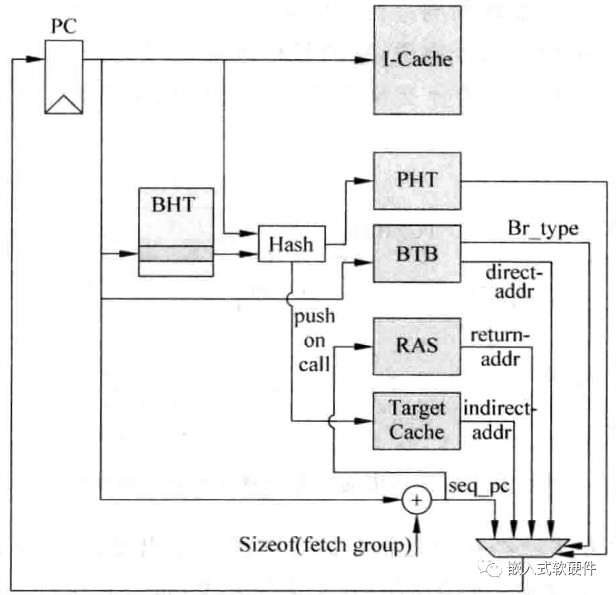
Dynamic prediction refers to predicting the future behavior of branch instructions based on their past performance during program execution, making predictions about the direction of program jumps and the target addresses. Typically, there are prediction mechanisms based on local information (BHT/PHT), global historical information (GHT/GHB), as well as BTB and RAS, forming a complete prediction mechanism. As shown in the example below:
BHT (Branch History Table)
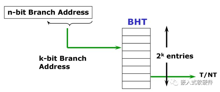
BHT is a local branch jump record, where each conditional jump instruction’s jump record is separately stored in dedicated displacement registers directly mapped by address. Based on historical prediction results and the current PC value, the counter table is read to predict whether the current branch is taken.
PHT (Pattern History Table)
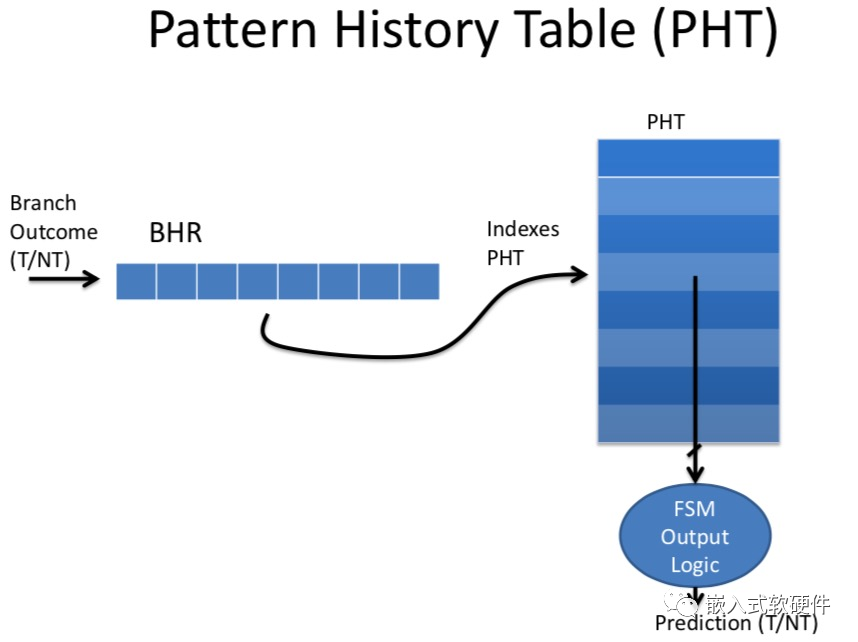
Branch prediction is generally based on the PC value. Considering that not all instructions are branch instructions, we usually take a segment from the middle of the PC as the address for storage or a table entry. This storage is called PHT (Pattern History Table). Typically, hashing methods are used to hash the PC value before addressing the PHT to reduce the issue of multiple branch instructions sharing a single PHT entry.Using the Branch History Register (BHR) can record the historical state of branch instructions, then using the value of the BHR as the index for the PHT allows predictions to be made for each historical state.It is also referred to as a two-level adaptive predictor based on local history:
-
The length of the branch history is N bits, used to record the branch direction of a certain branch for N times; -
The Pattern History Table has 2^N entries, each recording a state.
GHT (Global History Table)/GHB (Global History Buffer)
if(aa == 2) //b1
{
    aa = 0;
}

if(bb == 2) //b2
{
    bb = 0;
}

if(aa != bb) //b3
{
    some statements
}
If branches b1 and b2 are executed, then branch b3 will not be executed. Relying solely on the local history of branch b3 for prediction will never discover this pattern. Therefore, when predicting b3, it is necessary to consider the jump results of both b1 and b2 simultaneously, which can be addressed using GHT (Global History Table) or GHB.
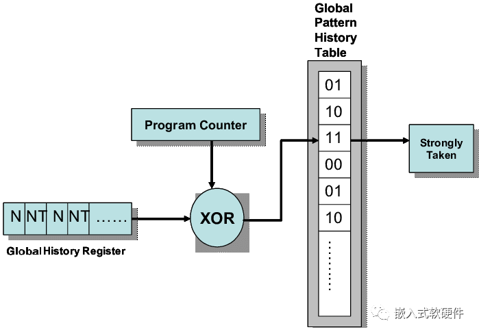
GHT is a global branch jump record, using the Global History Register (GHR) to record the jump results of several recent branch instructions. This Pattern History Table serves a similar purpose as the historical table mentioned earlier.It is also known as a two-level adaptive predictor based on local-global history. If the Pattern History Table is implemented as a FIFO structure, it becomes GHB (Global History Buffer). This can be understood in this way; we will not elaborate on the details.
BTB (Branch Target Buffer)
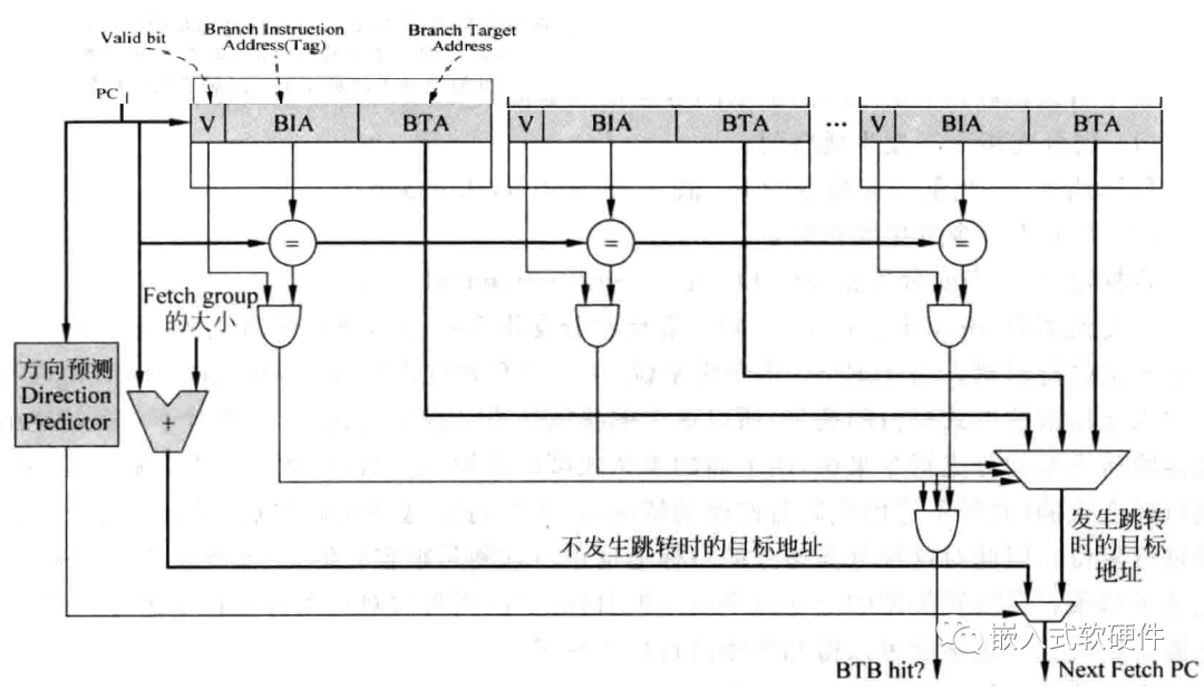
BTB records target addresses, similar to a cache. To save resources, BTB generally only records the target addresses of branch instructions that cause jumps; the target addresses of non-jumping instructions are simply the sequential instruction addresses. It uses part of the PC as the index for addressing, and other parts as the tag. The BTB stores the target addresses (BTA) of branch instructions. Using BTB can predict the target addresses of call instructions, often used in conjunction with RAS, and sometimes referred to as BTAC (Branch Target Address Cache). The following diagram is an example of a set-associative BTB:
RAS (Return Address Stack)
For indirect jumps like return, the target address is not fixed because multiple callers may call the same function. The CPU can set up a Last In First Out (LIFO) memory structure called RAS, which writes the address of the next instruction after the CALL instruction into RAS. This address is at the top of the stack, and when returning, it can be directly popped from the stack for the return target address. Using RAS can predict return target addresses.
Overall Review of Out-of-Order Execution Processors
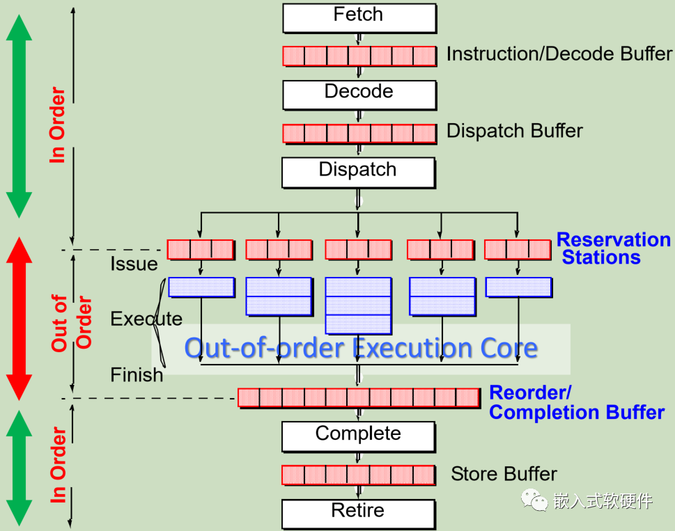
At this point, we can look at the overall picture of modern superscalar out-of-order execution, with each stage as follows:
-
Instruction Fetch & Decode: Sequential, speculative, due to Branch Prediction, I-Cache prefetch, and the existence of fetch buffers; -
Dispatch: Sequential, speculative, register renaming occurs at this stage, including allocating ROB (Reorder Buffer) entries and dispatching instructions to various functional units (FU) for execution. -
Issue: Out-of-order, speculative, after dispatching through the pipeline, instructions are written to the reservation station (Reservation Station, which can also be implemented as an Issue Queue or Instruction Window), and the arbitration circuit selects suitable instructions to send to the FU for execution. -
Execute: Various functional units execute out-of-order, with speculation. -
Commit/Retire: Ordered commit, without speculation, to achieve sequential instruction commit, the processor uses a buffer called the Reorder Buffer (ROB) to submit in the order of ROB, updating the results of relevant components, and finally placing memory access results into the store buffer, which are then written to main memory based on relevant policies.
Various Buffers
In a sequential execution core, instructions flow through each pipeline unit without needing caching. However, to enable out-of-order execution, a buffer is required to cache instructions that have not yet executed, and the execution order of these instructions is scheduled within this buffer, which is crucial for decoupling various components.
Register Renaming
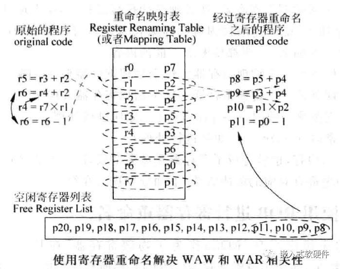
In processors that adopt out-of-order execution, register renaming uses a mapping table to map logical registers (as represented in instructions) to physical registers (the registers participating in operations within the processor). This resolves WAR and WAW dependencies, allowing independent instructions to execute simultaneously, increasing parallelism. As shown in the diagram:
ROB (Reorder Buffer)
ROB is essentially a FIFO that stores information related to an instruction, such as the type of instruction, target address, and whether it is valid. The capacity of the ROB determines the maximum number of instructions that can be executed simultaneously in the pipeline:
-
Provides a mechanism for undoing instruction execution -
Instructions are stored in the ROB in the order they are issued -
Instructions are committed in the order they are executed logically
Load bypassing and forwarding
These techniques optimize dependencies like Write After Read (RAW). Let’s take a brief look.
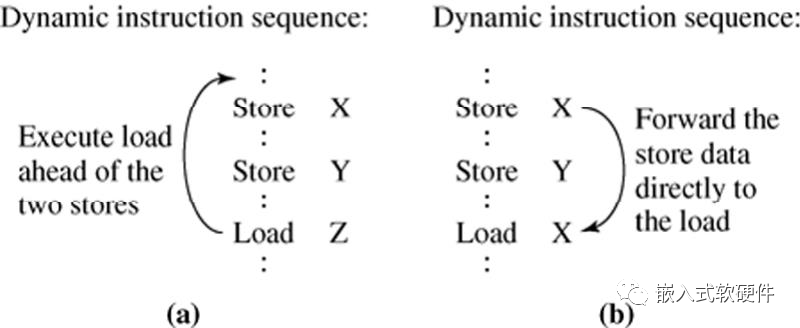
These two are data-oriented techniques (which can lengthen the critical path, making it unfavorable for increasing the main frequency). As shown in the diagram:
-
Bypassing (load bypassing): Under certain conditions, loads can be allowed to bypass stores and execute beforehand. Store data is retained in the ROB until the previous instruction completes, and is also kept in the store buffer until access permission for the cache port is obtained; -
Load Forwarding: If a pending load depends on store data in the store buffer, it can complete the load early without waiting for the store to be sent to the data cache. If both the load and store addresses are valid, and the data is available in the store buffer, it can be fetched directly from the store buffer, avoiding data cache access.
MMU

In addition to completing the mapping from virtual addresses to physical addresses, the MMU can also control the access permissions of each memory area (generally at the page size level), the order of memory, cache strategies, etc. With the MMU, application programs in the system are unaware of physical memory, and each application has its own independent and continuous virtual address space, improving memory usage efficiency.
The TLB (Translation Lookaside Buffer) is a high-speed cache within the MMU used to accelerate the speed of virtual-to-physical address translation. Without TLB, each data access would require access to the page table to obtain the physical address and its corresponding data.
Since the MMU is relatively familiar to everyone, and the internal structure of the TLB, ASID, page tables, etc., are related to CPU architecture, we will introduce them in detail in the next article on ARM architecture and microarchitecture.
Cache
This section will mainly introduce the basic principles and structures of cache, cache addressing methods, various cache strategies, ARM processor cache operations, memory attributes, PoC, and PoU concepts. We will cover these in subsequent articles.
Basic Concepts of Cache
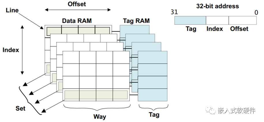
As shown in the figure, cache is generally set-associative. The 4-way set-associative cache shown above splits the address into three parts for easy indexing: Tag, Index, and Offset:
-
Line: A cache line is the smallest unit for exchanging data between cache and main memory; -
Tag: The highest part of the memory address, used to mark whether the data at this address is already in the cache. There is a separate Tag RAM in the cache to store these tags (not included in the cache line), and each tag corresponds to each cache line; -
Index: The middle part of the memory address, used to address which cache line to access; -
Offset: The middle part of the memory address, this part indicates the specific offset of the data in the current address within the cache line; -
Way: We divide the cache into multiple parts, each part is one way. Thus, a 4-way set-associative cache means the cache is divided into four parts; -
Set: The cache can be viewed as a two-dimensional matrix, where each element is a cache line. A row is a set, and the Index bits are used to locate a specific row (set). Each set consists of multiple cache lines. A 4-way set-associative cache means that each row (set) has four cache lines.
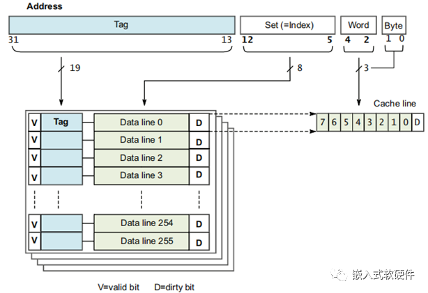
Let’s look at an example. In the figure above, a 32-bit address, a 4-way set-associative cache, and a cache line size of 8 words (32 bytes):
-
31-13 bits are the Tag field, totaling 19 bits; -
12-5 bits are the Index field, totaling 8 bits, with each way corresponding to 256 cache lines; -
4-0 bits are the Offset field, totaling 5 bits, where bits 4-2 can specifically locate which of the 8 words is being accessed; bits 0-1 can address which byte within each word (4 bytes) is being accessed;
Additionally, each Tag in the cache implementation has a V (valid) bit and each cache line has a D (dirty) bit (these two flags also occupy storage space):
-
Valid bit: Used to mark whether the data in the cache line can be used; -
Dirty bit: Used to mark whether the data in the cache line is consistent with the main memory.
Cache Organization Structures
Direct Mapping
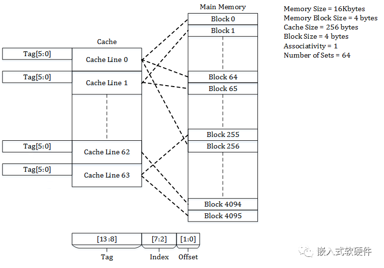
Direct mapping means that a block in main memory can only be mapped to a fixed row in the cache, as shown in the figure. Each set has only one cache line, resulting in 64 sets. Direct-mapped caches are simpler in hardware design and lower in cost but are prone to cache thrashing.
Set-Associative
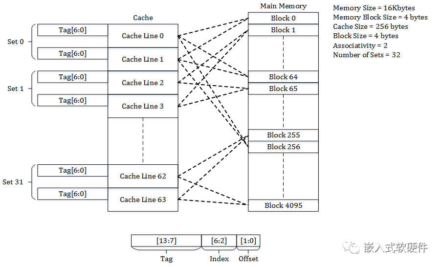
Set-associative means that a block in main memory can be mapped to a fixed set of rows in the cache. As shown in the figure, each set has two cache lines. There are 32 sets, and as long as one of the two is valid, a cache hit occurs. The hardware cost is higher than for direct-mapped caches but can reduce cache thrashing.
Fully Associative
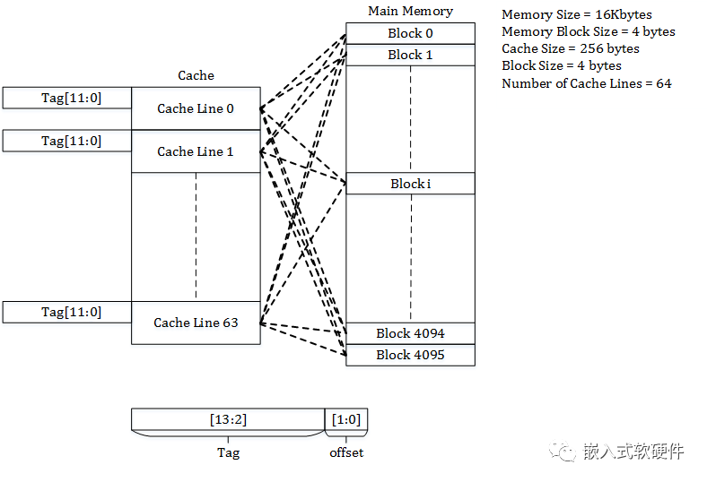
Fully associative means that a block in main memory can be mapped to any cache line in the cache, as shown in the figure. This means that all cache lines are within one set, so there is no need for a set index in the address. The hardware implementation cost is the highest, but it can minimize cache thrashing.
Cache Strategies
Allocation Strategies
-
Read Allocate: Cache lines are allocated only when the CPU issues a read request. If it is a write request and misses, the data is directly written to main memory, leaving the cache unaffected; -
Write Allocate: More accurately, it should be called the read/write allocation strategy. When there is a cache read or write and a miss occurs, a cache line is allocated for that data. This allocation strategy is typically used in conjunction with the processor core’s write-back strategy.
Update Strategies
-
Write Through: Modifications in the cache are propagated to the next level of storage, even on hits, avoiding consistency issues, but it is less efficient than write-back; -
Write Back: Only when a cache block is replaced is the modified data block written to the next level of storage. Not every write will cause a write operation to the next level of storage, but inconsistencies can occur.
Replacement Strategies
When a cache miss occurs, it is necessary to decide which cache line to replace. Common replacement strategies for set-associative and fully associative caches include:
-
Round-robin: Replace cache lines in the set in a round-robin manner. For example, for a 2-way set-associative cache, the first line in the set is replaced, then the second line, and then back to the first line, cycling through. -
Pseudo-random: Randomly replace a cache line within the set. For example, for a 2-way set-associative cache, randomly replace one of the lines. -
Least Recently Used (LRU): Replace the cache line in the set that has been used the least recently.
Having discussed the key features and working principles of processors, we will now briefly overview the microarchitecture of the ARM Cortex-A9 processor to see which technologies are used to enhance processor performance.
Microarchitecture of the ARM Cortex-A9 Processor
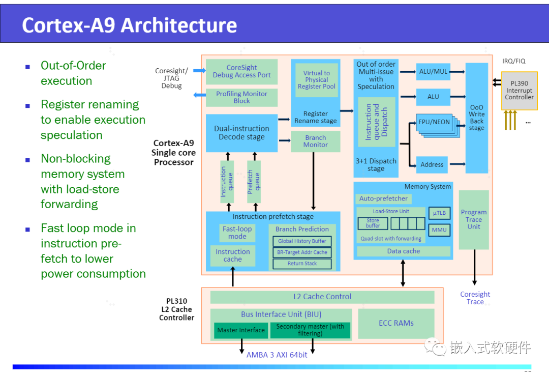
The Cortex-A9 is the first multi-core out-of-order processor from ARM. Let’s look at its features:
-
Instruction Fetch: Can fetch two instructions simultaneously:
-
Has one GHB to predict whether branches will jump; -
Uses BTAC (also referred to as BTB) to predict jump target addresses; -
Uses RAS to record function return addresses; -
Fast-loop mode: If it is a small loop with fewer instructions, it can avoid fetching data from the I-cache; -
Instruction cache: Configurable sizes of 16, 32, or 64KB; -
Decoding: Can decode two instructions per cycle;
-
Register renaming: Resolves WAR and WAW dependencies for out-of-order execution, improving efficiency and facilitating loop unrolling;
-
Dispatch & Issue: Can issue two instructions to the back end each cycle and dispatch four instructions to execution units (ALU/MUL, ALU, FPU/NEON, Load/store address generation units) each cycle. The instruction queue can choose instructions out of order.
-
Execution Units: Can execute concurrently;
-
Memory System:
-
Uses load forwarding to optimize RAW dependencies, enhancing out-of-order execution; -
Two-level TLB structure (Micro and Main TLB); -
Data prefetcher: Supports line fill requests of four cache line sizes; -
Store buffer: 4 x 64-bit, with data merge capability; -
Out-of-order write back
-
SCU (Snoop Control Unit):
-
External L2 Cache: Configurable sizes from 128KB to 8MB; 4 to 16-way set associative -
Coresight: Used for trace (PTM) & debug (connecting to the simulator’s DAP and performance monitoring PMU)
-
External GIC: PL390 (GICv1)
-
Bus Interface: Master0 & Master1, used for data and cache path data acquisition, AMBA3 AXI 2*64
The table below shows the detailed parameters of the A9 processor. In the next article, we will elaborate on these parameters and compare the microarchitectures.
| Feature | Feature | Cortex-A9 |
| General Information | Announced Date | 2007 |
| Release Date | March 2008 | |
| Type | Mainstream | |
| Design Team | Sophia-Antipolis | |
| Typical Clock Speed | ~2GHz on 40nm | |
| Multicore | 1-4 cores | |
| PPA | Peak Integer Throughput (DMIPS/MHz) | 2.5 |
| Power | < 250 mW@1GHz | |
| Performance Boost | >50% performance over the A8 | |
| Area | <=1.5 mm² | |
| Process | 40nm | |
| Main Extensions Information | Floating Point Unit | Optional |
| Half Precision Extension (16bit) | Yes | |
| Hardware Division | No | |
| Hardware Fused Multiply-Accumulate | No | |
| LAPE Extensions (40bit) | No | |
| Virtualization Extensions | No | |
| big.LITTLE | No | |
| VFP Architecture | VFPv3 | |
| NEON Architecture | NEON | |
| Pipeline | Execution Order | Out of Order |
| Pipeline Stages | 9-12 stages | |
| Instructions Decoded Per Cycle | 2 (Superscalar) | |
| Branch Prediction | BTAC (BTB) | A 2-way BTAC, implemented in RAMs with 512-4096 entries |
| GHT (Global History Table) | 1024, 2048, 4096, 8192, or 16384 2-bit GHB | |
| Other Predictor Components | – | |
| Return Stack | 8-entry | |
| MMU-TLB | Micro-TLB/L1 TLB (Instruction & Data) | 32-entry |
| Main-TLB | Fully-associative, lockable array of four elements; 2-way associative, 64-512 entries | |
| Cache | D$ Implementation | PIPT |
| I$ Implementation | VIPT | |
| L1 I$ Size (KB) | 16-64 | |
| L1 D$ Size (KB) | 16-64 | |
| L1 I$ Structure | 4-way set associative | |
| L1 D$ Structure | 4-way set associative | |
| L1 D$ Linefill Buffer Size (Bytes) | 2 * 32 | |
| L1 D$ Eviction Buffer Size (Bytes) | 32 | |
| L1 D$ Store Buffer Size (Bits) | 4-entry, 64 | |
| Replacement Policy (L1I$/L1D$) | Pseudo round-robin or pseudo random / pseudo random | |
| L2$ Structure | ? | |
| L2 Cache | External L2C-310 | |
| L2 Cache Size (KB) | – | |
| Cacheline Size (I$/D$, Bytes) | 32/32 | |
| ECC | None | |
| Others | ACP | Optional |
| Generic Timer | Private & Global Timer | |
| Interrupt Controller | Integrated GIC v1 (MP only), GIC-390 | |
| Bus Protocol | AMBA3 AXI 2*64 | |
| Trace | Integrated PTM |
This article is complete. In the next article, we will briefly introduce the architectural features of ARMv7-A and provide a more detailed exploration of this series of microarchitectures.
References:
-
Cache organization methods, smcdef -
Pipeline/Superscalar/cache placement policies, Wikipedia -
Computer Organization Principles – Principles Volume Processor (Part 1, 2, 3), wwj99 (Little Radish Duck), cnblogs (Blog Garden) -
Lecture 9: Modern Superscalar Out-of-Order Processors, Carnegie Mellon University -
Branch Prediction, TaigaComplex/Blog Garden -
Superscalar Organization – ECE/CS 752 Fall 2019, Prof. Mikko H. Lipasti University of Wisconsin-Madison -
ARM Cortex A9, Alyssa Colyette & Xiao Ling Zhuang -
ARM Cortex-A Series Programmer’s Guide for ARMv7-A, ARM Official Website -
ARM Cortex-A9 Technical Reference Manual, ARM Official Website