
Today, I will share knowledge related to OTG.
You can insert a USB flash drive into the development board, at which point the development board acts as a USB Host.
If the development board needs to communicate with a PC, it must act as a USB Device.
When the development board needs to act as both a USB Host and a USB Device, it can use the OTG port: it can automatically identify its role based on the hardware circuit and switch between USB Host or USB Device.
The OTG port comes in various forms, commonly Micro USB and Type C.
1.1 Micro USB
For the Micro USB socket, it has 5 pins:
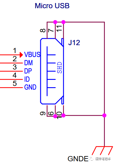
The function of the pins is shown in the table below:
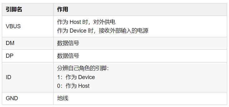
When the development board acts as a USB Device, it connects to the USB on the PC, and the PC’s USB interface only has VBUS, DM, DP, GND, so the development board’s ID pin is not connected to the PC’s USB port, it is pulled high by the pull-up resistor on the board.
When the development board acts as a USB Host, it needs to connect to an “OTG converter” and then connect to the USB flash drive.
The internal circuit of the OTG converter is very simple, it just pulls the ID pin low:
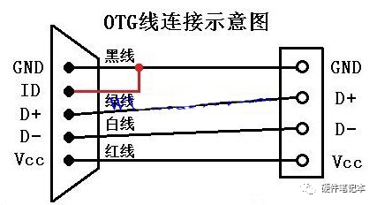
After this converter is plugged into the OTG port of the development board, the ID pin on the OTG port is pulled low, and the software converts the development board to USB Host.
1.2 Type C
The Type C socket has two sets of identical signals, and the Type C data cable can be used regardless of whether it is plugged in the right way or upside down.
The Type C socket has the following signals, and in the USB2.0 protocol, we only care about the signals in the red box:
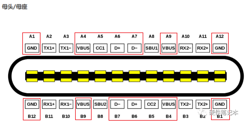
When the development board acts as a USB Device, it connects to the USB on the PC, and the PC’s USB interface only has VBUS, DM, DP, GND, so the CC1 and CC2 pins of the development board are not connected to the PC’s USB port, they are pulled high by the pull-up resistor on the board.
When the development board acts as a USB Host, it needs to connect to an “OTG converter”.
If we do not consider compatibility with the USB 3.0 protocol, the circuit diagram of the above converter is very simple, just connect the CC pins inside the Type C plug to GND through a 5.1K ohm resistor.
The OTG interface on the development board needs to achieve two functions:
-
Detect the ID pin (if using the Type C interface, it is the CC1 and CC2 pins), introduce the main control chip: the software sets the USB controller’s role (Host or Device) based on it
-
Decide whether to output power on VBUS based on the ID pin (or CC1, CC2): this is automatically achieved by the hardware circuit, or a dedicated chip can be added
2.1 Micro USB
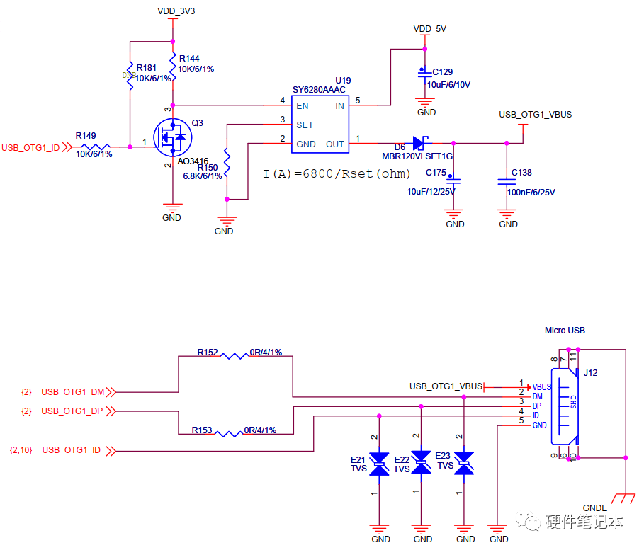
When USB_OTG1_ID is high, it indicates that the ID pin is pulled high by the board’s pull-up resistor, and it is not pulled low. At this time, AO3416 is turned on, and the EN pin is not enabled. Thus, SY6280AAAC will not supply power externally, and USB_OTG1_VBUS will have no voltage.
When USB_OTG1_ID is low, it indicates that the ID pin is pulled low, at which point AO3416 is turned off, the EN pin is enabled, SY6280AAAC supplies power externally, and USB_OTG1_VBUS has voltage, with the development board acting as a USB Host supplying power externally.
2.2 Type C
If we do not consider compatibility with the USB 3.0 protocol, we can use the following simplified circuit: CC1 and CC2 as ID pins. The principle is similar to the above diagram.
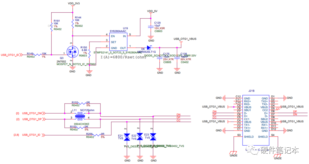
If we want to be compatible with the USB 3.0 protocol, we need to add a dedicated chip, which detects the status of CC1 and CC2, sends an interrupt to the main control, and reports the information to the main control through I2C, allowing the main control to control the power supply pins:

4. https://blog.csdn.net/qq_37659014/article/details/124479125
Disclaimer: This article is sourced from the internet. Reproduction is for learning reference only and does not represent the views of this account. This account also does not bear any copyright responsibility for its content, text, or images.