
AI applications on terminal devices (mobile phones, cars, robots, etc.) are divided into training and inference stages.
Training is generally done on servers using NVIDIA graphics cards, which are still a reliable way to obtain ultra-large computing power. The models obtained from training are deployed to terminal devices, which use information captured by sensors such as cameras and microphones to perform inference, resulting in intelligent outcomes, such as smart photography on mobile phones and autonomous driving in cars.
Inference requires less computing power and is highly customizable, making it technically less challenging. Therefore, specific industry sectors can develop their own solutions, such as Horizon and Tesla’s autonomous driving AI chips. Of course, NVIDIA has also ventured into some popular fields, such as the Orin autonomous driving chip, but it does not dominate the inference chip market like it does in training chips. Inference technology is the easiest, and there is an explosive trend in the domestic market. Basically, any listed company with some strength is developing AI chips, which are essentially AI inference chips. However, giants like ByteDance, Tencent, and Alibaba, which lack terminal devices, can only develop cloud inference or training chips.
In summary, AI inference SoC chips are undoubtedly a focal point in the current chip field. This article directly approaches the topic from a technical perspective, unveiling the architecture of AI SoC chips with plenty of valuable insights. Feel free to share it with friends for reading!
1. AI Inference SoC Chip Architecture
1.1 Huawei Da Vinci
Reference: ZOMI Sauce’s “AI System” Bilibili video: www.bilibili.com/video/BV1Ls…
In previous articles: AI System – 15 Introduction to Domestic AI Chips, which provided some information but not in detail or from an architectural perspective, this article will break it down.
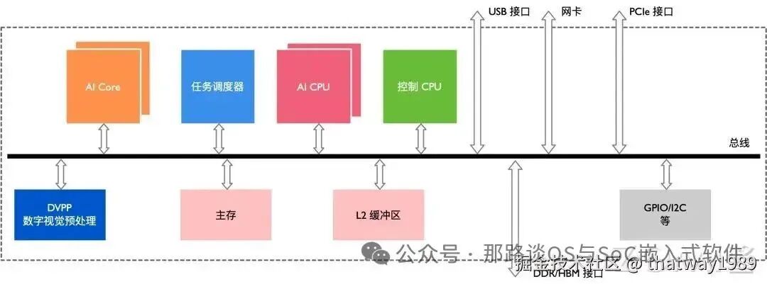
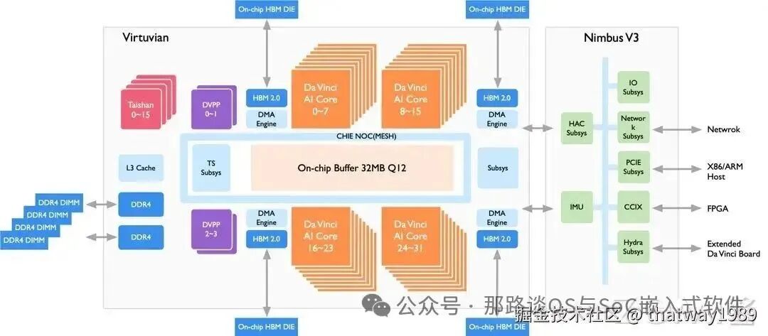
From the above two images, we can see the composition of the AI chip:
- CPU: Runs user interaction programs, collects AI tasks here, and issues commands to the NPU for computation. This is generally an ARM A-core CPU.
- NPU: The Da Vinci AI core here is the NPU responsible for processing neural network computation tasks.
- Cache: Composed of SRAM, serves the NPU, stores data for NPU computation, relatively fast and expensive, measured in M.
- NoC: On-chip network, fast transmission speed.
- DMA: Assists in data transfer for the NPU, freeing the AI core for computation.
- DDR: Stores data collected by the terminal, such as audio and video, slower than SRAM but larger in capacity, measured in G. HBM can also be used here for faster speeds.
- Task Scheduler TS Core: A hardware module that shards AI tasks and distributes them in parallel to the NPU for processing, generally an ARM M-core or RISC-V.
- ISP: DVPP, preprocesses video data before sending it to the NPU for processing.
- SPI flash: Stores the firmware program for system operation, usually an fip package under ARM, measured in M. This is an external device to the SoC, with a controller inside the SoC.
- UFS: Stores the Linux image and file system, large capacity, serves as system memory, measured in G. This is also an external device to the SoC, with a controller inside the SoC.
- Peripherals: USB, network cards, PCIe, GPIO, I2C, SPI, UART, etc., divided into high-speed and low-speed devices, also external devices to the SoC, with a controller inside the SoC.
1.2 Tesla FSD Chip
Reference previous article: AI System – 14 Tesla FSD Chip
 Directly looking at the composition of the AI SoC chip:
- CPU: Uses ARM A78, mainly responsible for issuing commands for AI tasks.
- NPU: Uses two NPUs for hardware-assisted acceleration of AI tasks.
- LPDDR: Main memory, relatively low power consumption.
- NoC: On-chip network, the fastest communication within the SoC, mainly connecting DDR and SRAM for large data transfers, as well as various subsystems.
- ISP: Graphics processing, video data needs preprocessing before being sent to AI for computation.
- VPU: Video encoding and decoding, mainly for compressing and decompressing video data when storing and uploading to the cloud. This is where user data is sent back to the product company, which uses this data to train larger and better models. The competition in the AI field is about who has more data and stronger algorithms for greater accuracy.
- Video Interface: The interface between the camera and the SoC, generally using MIPI to transmit video data from the camera to the SoC, where the ISP preprocesses the data before sending it to the NPU for inference. Meanwhile, the VPU will also upload some data to the cloud via 5G.
- Functional Safety Subsystem: FSI, emphasizes safety in the automotive field. This module mainly checks for functional failures in the SoC and provides timely remedies.
- Information Security Subsystem: HSM, integrates some data encryption and decryption modules for security verification, such as secure boot verification and user core data (password login) verification.
- GPU: This was later removed, likely because the initial NPU could not handle it, and after collaborating with NVIDIA, they learned some things and then abandoned it.
1.3 NVIDIA Orin
Reference: NVIDIA ADAS – Introduction to NVIDIA Orin Chip
Also: www.nvidia.com/content/dam…
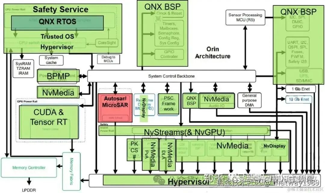
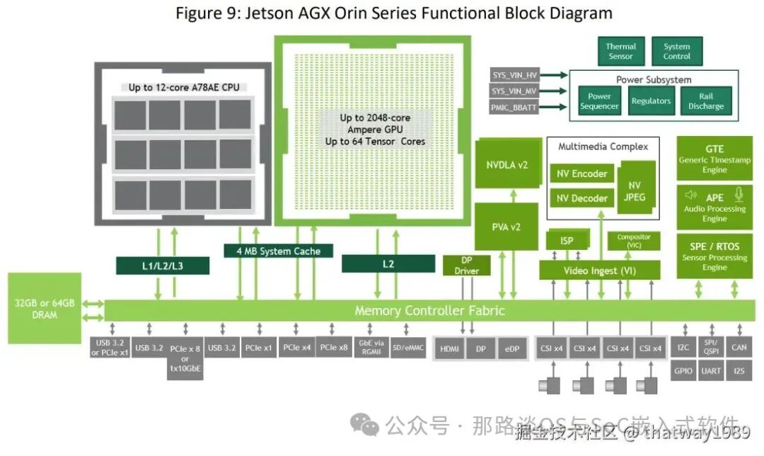
From the above images, we can directly analyze its composition:
- CPU: Uses A78E, which is a safety architecture A-core designed by ARM for automotive applications. The software RTOS is likely using QNX BSP.
- GPU: Uses Tensor Cores, which are specialized cores within the GPU that have been customized to function as an NPU.
- Cache: Multi-level cache, similar to CPU design principles.
- LPDDR5: Main memory.
- QSPI FLASH: Firmware storage.
- Memory Controller Fabric: Manages memory access. It does not use efficient NoC; instead, it uses various caches, directly accessing data in DDR.
- ISP: Image preprocessing.
- Power Management System: Clock, reset, power monitoring.
- FSI: Functional safety, using ARM R52 core, achieving ASIL D level.
- Information Security: HSM also uses ARM R52, mainly managing encryption and decryption hardware and trust roots like eFUSE.
- AUTOSAR: Vehicle control-related systems.
- Hypervisor: Because multiple OS run on heterogeneous cores, such as QNX and AUTOSAR OS, a virtual machine is needed.
- High and Low-Speed Peripherals: PCIe/CAN/SPI/I2C/GPIO/UART controllers.
2. AI Inference Chip SoC Design
When designing an AI SoC, the first step is to modularize based on requirements, starting with what we need.
- Select CPU based on performance and safety requirements.
- If image processing is needed, then ISP, NPU, and VPU are required.
- If functional safety is needed, then FSI should be used.
- If information security is needed, then HSM should be included.
- Power management and system control for multiple subsystems need to be separated, requiring SCP.
- Storage requires UFS, SPI FLASH, DDR, SRAM, etc.
- Communication involves NoC, AXI, and various communication buses to connect these sub-modules.
- Heterogeneous core business subsystems, such as AUTOSAR in vehicles, ideally integrate all product systems into one SoC, which represents an upgrade in product-level electronic architecture.
Each subsystem mentioned above may represent a team in actual R&D. Even if an article introduces one, it only scratches the surface. Future articles will attempt to provide more detailed introductions. Here, we will first look at some points to pay attention to in general chip design.
2.1 Memory Mapping
As a software engineer, the most intuitive aspect of hardware is the register addresses. How these addresses are uniformly planned and what each subsystem’s base address offsets mean need to be looked at in the chip manual.
Generally, chips provide three manuals:
- User Manual: Environment setup, software burning, etc., explaining how to use the system without involving coding and compilation.
- Development Manual: Introduction to SDK code framework, compilation, and various module configuration modification methods.
- Reference Manual: Overall chip parameters and register descriptions.
Memory Mapping is about planning the use of the entire system’s addresses, like the address numbers for the entire system:
- Specifies which address range belongs to which subsystem, and each subsystem also has its own memory layout.
- Different subsystems may see different addresses.
- For system security needs, addresses are divided into secure and non-secure worlds.
- Addresses typically start with some cfg configuration-related ones, followed by SRAM and then DDR memory-related addresses.
- Addresses are generally divided into device attributes and memory attributes, controlled by certain hardware like MPU and TCM for access settings regarding storage, as follows:
- SRAM is more efficient than DDR. Generally, subsystems are configured around it based on needs for firmware storage, inter-core communication, information scheduling, and storing information during sleep.
- efuse is one-time programmable storage for storing keys.
- LPDDR is low-power double data rate dynamic random access memory.
- Flash storage.
- UFS stores system programs and application data.
- TCM: In ARM Cortex processors, TCM is a type of high-speed memory located next to the processor core, designed to provide low-latency and high-bandwidth memory access performance. Accessing memory in TCM is usually faster than accessing regular RAM or cache.
- MMU is used for address mapping.
- DDR interleaving: Allocates consecutive addresses to different DDR chips, improving DDR bandwidth and utilization.
The address ranges seen by 32-bit and 64-bit heterogeneous processors are different, so different mappings are needed.
2.2 On-Chip Communication in SoC
2.2.1 Introduction to Bus Development
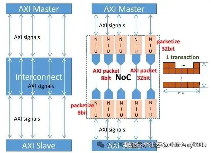
The flow of data mainly relies on the I/O bus in the system-on-chip, such as the AMBA standard provided by Arm in the image above. Using a DMA controller allows external data to be directly transferred to memory without going through the central processor, greatly improving data throughput efficiency.
In the past decade, a trend in SoC design has been to adopt network-based topologies to improve on-chip communication efficiency. This routing-based packet interconnect network is called “on-chip network” (NoC), which can overcome the bandwidth bottlenecks of traditional bus networks.
What are the advantages and disadvantages of NoC compared to traditional bus interface communication?
As the number of IP modules in SoC continues to increase, the complexity of on-chip quality of service (QoS), arbitration, and data flow optimization is also rising. NoC is gradually replacing buses and crossbars as the industry standard for on-chip interconnect. Buses are shared communication resources, and beyond the simplest systems, buses cannot provide the bandwidth required by the system. Crossbars can provide sufficient bandwidth, but their size grows exponentially with the number of connected IP modules, and large crossbars are practically impossible to construct. They also do not utilize wiring well, which is the most expensive aspect of today’s chip technology. NoC can greatly reduce die area (especially with less wiring), lower power consumption, and can fine-tune and optimize on-chip data flow and quality of service, even providing data protection features to enhance the overall system’s functional safety.
Buses were the standard used in the early stages of system-on-chip development when the number of connected IP modules (CPU, memory, peripheral controllers, etc.) was typically fewer than 20. However, as more IP modules connect to the bus, they begin to compete for priority and available bandwidth. Buses require centralized arbiters and address decoding logic, and as the number of masters and slaves increases, they compete for the same bus resources, which becomes a bottleneck for SoC performance.
- NoC buses can connect to subsystems via AXI, APB, etc. Accessing data through the bus can lead to data consistency issues in multi-core systems, which will be discussed in a later topic. The most typical case is that A-cores access other hardware like LPDDR and SRAM through NoC, requiring a hardware module like CMN600AE between the A-core and NoC.
- For subsystems with high bandwidth requirements, such as AI subsystems that need to process large amounts of camera and multimedia data, dedicated channels should connect to NoC to avoid competing for NoC resources with other subsystems.
- Through NoC, configuration registers and data registers can be accessed. For example, accessing the ISP’s registers from an A-core requires going through NoC.
2.2.2 ARM’s CI-700 and Arteris NoC
NoC is structurally divided into Request Path and Response Path, with each Path containing NIU, switch, link, reorder buffer, etc. Here are two commonly used solutions: ARM’s CI-700 and Arteris NoC
Reference: blog.csdn.net/ygyglg/arti…
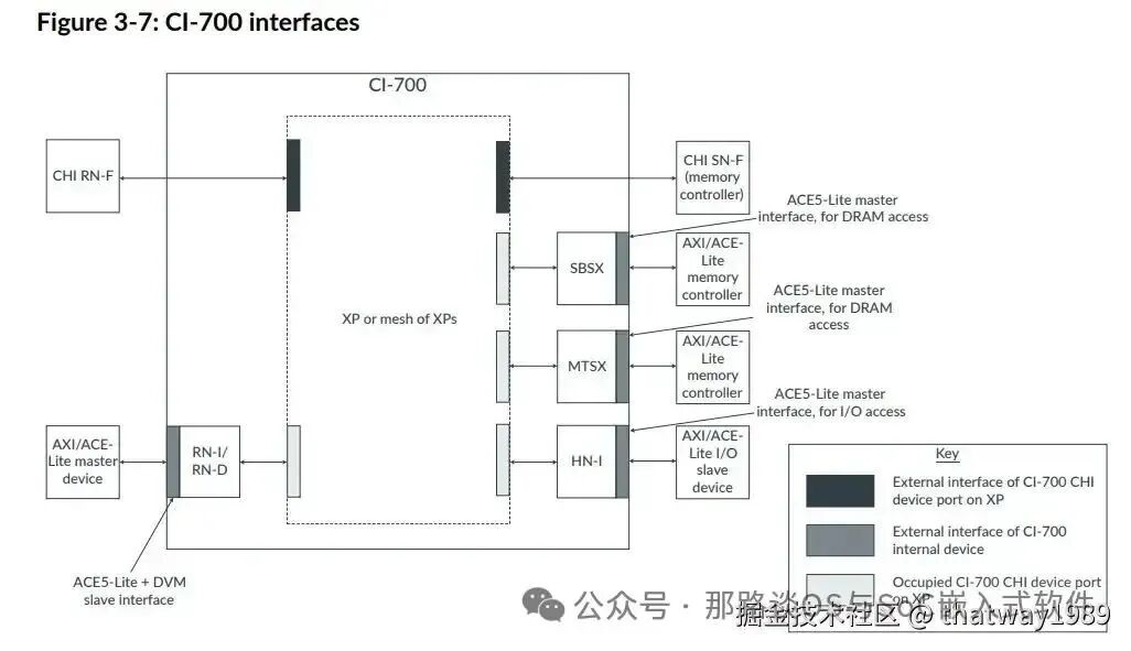 ARM’s CI-700:
- AMBA 5 CHI interconnect: CI-700 is a connection technology based on AMBA 5 CHI (Coherent Hub Interface), designed for mobile and client SoCs, providing high performance and low power solutions.
- Customizable mesh topology: CI-700 supports customizable mesh topologies, allowing designers to optimize network structures based on specific SoC needs for the best performance and power balance.
- Supports Armv9 processor design: CI-700 is compatible with the Armv9 processor architecture, capable of supporting the new generation of high-performance computing needs.
- System-level cache: CI-700 introduces the concept of system-level cache, which can improve data transfer efficiency, reduce access to external memory, and thus lower system power consumption.
 Arteris NoC:
 - FlexNoC 5: Arteris’s NoC technology, represented by FlexNoC 5, is an indispensable IP generator for efficient, high-performance NoC design.
- Physical awareness: FlexNoC 5 has advanced physical awareness capabilities, providing intuitive design feedback early in the design cycle, accelerating timing convergence, reducing area, and providing a good starting point for physical layout teams.
- Supports multiple protocols: Arteris’s NoC supports various protocols, including AMBA 5 ACE-Lite, AHB, AXI, etc., making interoperability between IP blocks more flexible.
- Functional safety: FlexNoC 5 offers FuSa options, supporting functional safety up to ASIL D level, suitable for high-safety automotive and industrial applications.
Comparison Summary
- Design philosophy: CI-700 focuses on providing customized interconnect solutions for mobile and client SoCs, while Arteris’s NoC emphasizes flexible, configurable network interconnect technology suitable for various application scenarios.
- Performance and power: CI-700 optimizes performance and power through system-level cache and mesh topology, while Arteris’s NoC enhances performance and reduces power through physical awareness and multi-protocol support.
- Functional safety: Arteris’s NoC provides functional safety support, which is particularly important for automotive and industrial applications, while CI-700, although also concerned with safety, does not explicitly mention functional safety support.
- Interoperability: Arteris’s NoC supports a wider range of protocols, making it easier to interoperate with different IP blocks, while CI-700 focuses on compatibility with Arm processor architectures.
- When choosing suitable on-chip network interconnect technology, designers need to make decisions based on the specific needs of the SoC, expected application scenarios, and requirements for performance, power, and safety.
Both ARM’s CI-700 and Arteris’s NoC provide on-chip network interconnect solutions for SoC design, but they differ in design philosophy and target applications.
CI-700 is designed based on ARM’s AMBA 5 CHI interconnect standard, optimized for mobile and client SoC application scenarios. It features a customizable mesh topology that allows adjustments to the network structure based on SoC needs to achieve high performance and low power goals. CI-700 is compatible with ARMv9 processor architecture, supporting new generation computing needs, and introduces system-level cache to improve data transfer efficiency and reduce system power consumption.
On the other hand, Arteris’s NoC, particularly FlexNoC 5, is an efficient, high-performance NoC design with physical awareness capabilities that provide intuitive feedback early in the design process, helping to optimize interconnect structures, reduce development time and chip area, and lower power consumption. Arteris’s NoC supports multiple protocols, including AMBA 5, and offers functional safety support, suitable for high-safety automotive and industrial applications.
Overall, CI-700 focuses on tight integration with ARM processor architectures and optimized solutions for mobile SoCs, while Arteris’s NoC provides broader protocol support and functional safety features, suitable for various application scenarios. Designers should decide which technology to use based on the specific needs and target applications of their projects.
ARM’s manuals are publicly available:
developer.arm.com/search#numb…
Arteris requires account registration for downloads.
2.3 Clock and Reset
The clock is generated by PLL.
- Different subsystems require different clock frequencies, necessitating multiple PLLs.
- Modules with functional safety requirements, such as FSI, need separate PLLs.
- Modules in the AON domain also require separate PLLs, as they need to run independently during system sleep.
- DDR, as a high-speed interface, has high stability requirements and complex internal structures, requiring multiple PLLs to prevent clock skew and provide greater clock supply flexibility.
- PLLs exist in the CRU and are part of the CRU.
Regarding power domains and voltage sources:
- Design voltage domains based on different voltage requirements.
- Design power domains based on different subsystem functions.
- AON (Always On) is a power domain that remains powered.
- PIMC controls the power switch.
Reset:
- Controlled by CRU, a subsystem like FSI or SCP has an independent CRU to control its internal hardware modules, allowing register operations.
- The entire chip system has a TOP CRU to control the reset of each subsystem.
- DDR has multiple PLL controls and multiple CRUs to control reset states, providing greater flexibility.
- CRU includes PoR (Power-On Reset) to monitor power.
- The overall reset can be triggered by an external button or special GPIO signals, or by a software reset triggered by registers. Some subsystems require higher permissions, such as only FSI or SCP can trigger resets, while A-cores and other subsystems cannot.
- The watchdog WDT can also trigger resets.
For different power modes, such as sleep mode, energy-saving mode, and shutdown mode, some hardware functions need to be turned off, which requires using CRU to control these hardware’s clock and reset signals. For secure resets, application data must be cleared first, especially data transmitted over the NoC, before performing reset operations.
In ARM solutions, PLLs are typically integrated into the SCP subsystem, which is the System Control Processor, responsible for controlling the clocks and reset operations of various subsystems. The system’s sleep-wake process is also mainly completed independently in the SCP. Of course, if SCP is not needed, it can also be done in ATF’s BL31.
Different scenarios have different solutions. In fact, power management, information security HSM, and functional safety FSI are distributed across three small cores, but they can be unified using one or two cores. However, this poses challenges for software and hardware security, and handling it well is also possible.
Below is an example of a system integrating SCP:
For SoC sleep:
- The A-core needs to save its data and programs to DDR.
- DDR training data is saved to AON’s SRAM.
- Important system data is also saved to AON’s SRAM.
- The main control core (usually the A-core) notifies other subsystems to enter sleep mode.
- SCP controls the PPU to enter low-power state.
- SCP controls PMIC to power off some hardware.
- SCP controls PLL to turn off some clocks.
- SCP itself enters WFE low-power mode waiting for wake-up.
Wake-up:
- The wake-up source wakes SCP from WFE.
- SCP controls PLL to provide clocks.
- SCP controls PMIC to power on.
- SCP controls PPU to exit low-power mode.
- SCP notifies the main control core to exit sleep mode.
- The main control core notifies other subsystems to exit sleep mode.
- DDR restores the state and continues running.
Power-up and Power-down Timing:
- Power-up sequence must follow the voltage domain order.
- Must strictly follow the power-up sequence, and the time intervals must meet requirements.
Secure reset: For the secure reset requirements of subsystems, clear the communication data on their buses and securely shut down the internal subsystems. Here is an example of clearing the NoC:
- First, SCP needs to initiate a NoC clear request for the subsystem to be reset.
- After NoC replies with an acknowledgment, SCP can proceed with the reset. Other ADB/APB LPI Q-channel clear operations are similar.
Internal Secure Reset of Subsystems
- The core needs to enter WFI before resetting, so that in WFI state, most clocks are off, allowing for a secure reset.
- Alternatively, the core can control itself to enter low-power mode via the LPI bus before shutting down, avoiding system errors.
2.4 MailBox Communication
Reference previous articles: SoC Software Technology – Inter-Core Communication
Power Management Introduction – 5 arm-scmi and mailbox inter-core communication
NoC solves the communication access mechanism for hardware modules, allowing a subsystem core to access a specific location. However, when multiple subsystems work together, they need to inform each other to access that location. This is the inter-core communication MailBox, specifically for notification, as data is not sent directly but placed somewhere, notifying the other party to retrieve it.
- Data is placed somewhere, usually in shared memory or within the MailBox hardware.
- Hardware interrupt lines trigger the other party’s interrupt notification.
A MailBox can have multiple Channels, supporting many communication paths simultaneously. Channels are also divided into secure and non-secure paths, and the receiver needs to classify messages from these two types, discarding any secure requests received on the non-secure path.
2.5 Main Hardware Modules of Subsystems
Each subsystem in the SoC, such as SCP, FSI, HSM, and business-related ISP, NPU, VPU, has its own cores and OS. Hardware design is needed around the cores, along with corresponding business peripherals.
2.5.1 Interrupt Control
For heterogeneous cores, such as A-core (GIC), M-core (NVIC), R-core (GIC), RISC-V core (PLIC), each has its own interrupt controller hardware.
The chip manual needs to provide the interrupt vector table for each core, facilitating software functional development. During software debugging, interrupt numbers are often used to locate which module has issues.
2.5.2 DMA Hardware
DMA can connect to the bus via AXI, APB, etc. Generally, hardware is needed for large data transfers, such as between A-core and NPU.
2.5.3 Watchdog WDT
Each subsystem needs to have a built-in WDT to reset the subsystem in case of a hang or report events to the security center for handling.
Generally, WDT supports two levels of events. The first level is for the subsystem to handle itself, while the second level is for when the subsystem has hung and cannot handle events, reporting to the external system for processing.
2.5.4 Timer
To implement timed interrupts and time-related functions, subsystems need to have built-in Timer hardware.
2.5.5 RTC
Real-Time Clock (RTC) provides clock calendar functions.
2.5.6 Debugging and Tracing
Generally, a host computer needs to use JTAG or USB to debug and trace the chip.
- Debugging Architecture
- ARM CoreSight: ARM CoreSight is a set of advanced debugging and tracing technologies provided by ARM, designed for complex SoC designs. Among them, SoC-400 is a solution in this technology series, providing system-level debugging and tracing capabilities, supporting multi-core and cross-SoC debugging, with advanced debugging features like breakpoints and watchpoints, and can trace the instruction flow, data flow, and system events.
- Debugging Tools
- JTAG/SWD Interface: JTAG (Joint Test Action Group) and SWD (Single Wire Debug) are two commonly used debugging interfaces that allow developers to access the internal registers, memory, and perform debugging operations on the SoC through boundary scan or single-wire debugging connections.
- Debugger: Professional debugging software, such as ARM’s Keil MDK, IAR Embedded Workbench, etc., provides a graphical debugging interface, supporting breakpoint setting, single-step execution, variable viewing, and other debugging functions.
- Tracing Technologies
- Instruction Tracing: Tracing the sequence of instruction execution in the SoC helps understand the program’s execution flow and performance bottlenecks.
- Data Flow Tracing: Tracing data transfers between processors or between processors and external devices helps identify errors or performance issues in the data path.
- System Event Tracing: Recording system events in the SoC, such as interrupts, exceptions, DMA transfers, etc., for analysis during debugging.
2.5.7 PVT
PVT is used to sense changes in chip processes and operating environments, including the following types of sensors:
- Thermal Sensing (TS): High-precision thermal sensing, easy to integrate. Supports power optimization and reliability.
- Distributed Thermal Sensing (DTS): Distributed thermal sensing. Supports thermal mapping, highly precise placement, low latency.
- Supply Monitoring (VM): Power supply monitoring, measuring power voltages across multiple domains, verifying distribution networks, implementing static and dynamic IR drop analysis.
- Process Monitoring (PD): Process monitoring, understanding wafer speed changes (slow, fast, typical) during mass production or the lifecycle of a single chip. Provides power optimization and aging monitoring.
The PVT-Controller collects PVT temperature data and generates interrupts to obtain temperature data. If the temperature data exceeds the limit, it will report to higher-level subsystems like FSI for decision-making, which may lead to system shutdown.
2.5.8 Pin Control and Pin Multiplexing
The chip needs to provide pin multiplexing rules.
Most SOC pins support multiplexing, for example, the GPIO1_IO03 of I.MX6ULL can be used as a regular GPIO or as I2C1’s SDA, etc. Additionally, we need to configure the electrical characteristics of the pins, such as pull-up/pull-down, speed, drive capability, etc. The traditional way to configure pins is to directly manipulate the corresponding registers, but this method is cumbersome and prone to issues (such as pin function conflicts). The pinctrl subsystem was introduced to solve this problem, and its main tasks include:
- Obtaining pin information from the device tree.
- Setting the pin’s multiplexing function based on the obtained pin information.
- Setting the pin’s electrical characteristics based on the obtained pin information, such as pull-up/pull-down, speed, drive capability, etc.
For users, they only need to set the relevant attributes of a pin in the device tree, and all other initialization work is done by the pinctrl subsystem. In Linux, the source code directory for the pinctrl subsystem is drivers/pinctrl.
2.5.9 SRAM
SRAM is a relatively fast storage method that can be used for:
- The location of firmware execution, including various program segments, data segments, stacks, etc.
- Shared memory can be used.
- Storing system data, such as warm reboot parameters, configurations, etc.
- Data that needs to be preserved during sleep must use AON’s SRAM.
2.6 Security Design
TrustZone divides the system’s resources (via register addresses) into secure and non-secure worlds.
Some hardware and data can only be accessed by the secure world. Linux applications cannot access them directly; they must go through system calls to the kernel and then to secure subsystems like BL31 or SCP to perform operations on secure registers. This way, Linux applications can only access fixed interfaces, not exposing all registers, thus ensuring security.
- BL31 and OPTEE are in the secure world.
- SCP and FSI are in the secure world.
- DDR and SRAM can partially be secure world addresses and partially non-secure, requiring hardware like TZC or APB Filter for configuration protection.
- NoC distinguishes between Secure slave and non-Secure slave.
- DMA can be configured to access secure space.
2.7 SoC Boot Design
2.7.1 Introduction to Secure Boot
Refer to previous articles:
- Secure Boot Introduction – 8 Hardware Discussions and Summaries
- ATF: Introduction to ATF – 4 BL31 Boot Process Analysis, etc.
This section is about secure boot.
- Needs to support the ATF password verification process and BL1 booting from the chip’s ROM.
- Verification requires support from the CM hardware module.
- BootROM’s startup has startup modes that can be configured via efuse and pins.
- Key storage requires eFUSE support.
- fip package storage requires UFS’s QSPI FLASH support.
- Supports XIP, secure recovery, secure configuration, secure debugging, diagnostics, and other modes.
- Supports AB partitioning, lifecycle management, boot logs, and other functions.
Common DIP switch and pin configurations:
- Forced recovery mode: Boot from UFS.
- USB boot mode: Boot from USB download.
- XIP boot: eXecute In Place (chip-internal execution) booting means the chip can execute program code directly in non-volatile memory (like Flash) without first copying the code to RAM.
2.7.2 Boot Example
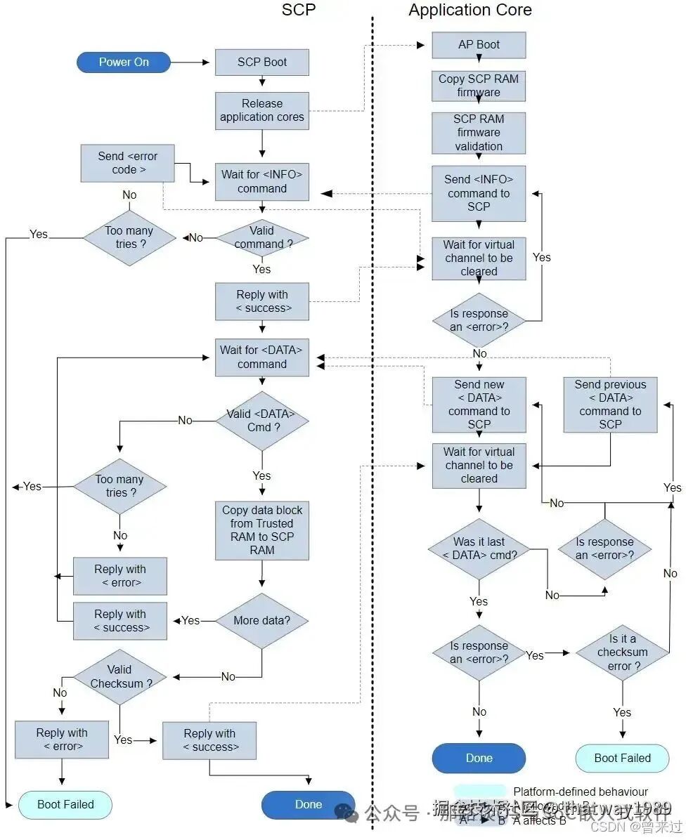
The above image is a flowchart of the SoC boot process based on ARM SCP:
SCP_BL1 boot process:
Upon system startup, the scp_romfw firmware code runs first. It executes the initial process of the scp application initialization, fwk_arch_init(), initializing interrupts, and modules in the order defined in Firmware.cmake. After these are completed, it will loop to handle runtime event messages.
ATF loads SCP_BL2:
TF (Trusted Firmware) is ARM’s security solution introduced in Armv8, providing an overall solution for security. It includes privilege level divisions during the boot and runtime processes. The main responsibility of ATF BL2 is to load subsequent firmware such as u-boot, kernel, SCP, or other heterogeneous core firmware into RAM. The loading and booting of SCP firmware is handled by ARM Trusted Firmware-A (TF-A).
SCP is responsible for power, clock, reset, and system control. BL2 loads the optional SCP_BL2 image from the platform storage device into a specific secure memory area. Subsequent processing of SCP_BL2 is platform-specific and needs to be implemented independently. For example, in Arm Juno:
- BL2 first loads SCP_BL2 into trust SRAM.
- Then uses Boot Over MHU (BOM) protocol to load SCP_BL2 into SCP’s internal RAM.
- SCP runs SCP_BL2.
- SCP signals the AP to notify BL2 to continue execution.
In ATF, the compilation options for BL2 are defined in plat/arm/board/juno/platform.mk under BL2_SOURCES. In morello ATF plat/arm/board/morello/platform.mk, BL2_SOURCES is not defined, and BL2 is not included. Whether to include BL2-related common code and configurations is determined by CSS_LOAD_SCP_IMAGES. For SCP code analysis, refer to: ARM SCP Introduction – Framework Code Analysis.
Postscript:
There is a lot of content in AI SoC chips, and large companies spend hundreds of millions to develop them, requiring large teams. The software and hardware R&D involved is complex, and future articles will begin to introduce them one by one, starting with the powerful NPU. Stay tuned!
“I understand a little about everything, but I am not proficient in anything,
I can do anything, but I am not good at anything,
Professionally, I am a jack of all trades, master of none.”
Welcome to leave messages if you have your own public account: Apply for Reprint!
Purely valuable content will continue to be updated, feel free to share with friends, like, collect, view, underline, and comment for communication!
Bonus:
-
This public account provides a WeChat technical exchange group to discuss automotive software technology together (first add WeChat: thatway1989, and note the technical direction of interest).
-
If you need advertising, business cooperation, you can also contact the author.