😶🌫️ Always staring at the phone So dizzy! 😇 Click 🎧 to listen and let’s sharpen our ears together 👂
How to unveil the “black box” of a chip without damaging the silicon wafer?
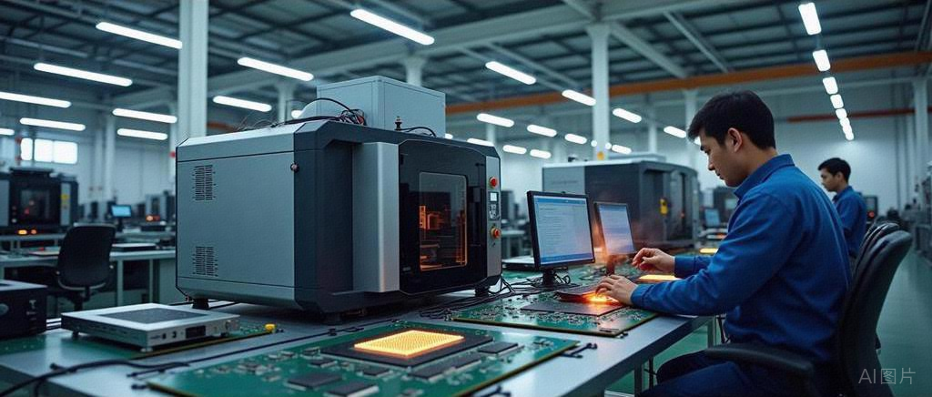
Chip decapsulation is a critical step in failure analysis, requiring precise removal of packaging materials at the micron scale while protecting the internal circuit structure. This article will reveal the core logic of this precision technology based on semiconductor physics and chemical etching principles, combined with the mechanical design of industrial-grade decapsulation equipment.
1. Process Principles and Technical Route
Why can’t traditional mechanical decapsulation meet the needs of modern chip analysis?
-
Dominance of Chemical Etching:
- Etching rate: 50-100μm/min (requires temperature PID control ±1℃)
- Safety protection: Acid mist collection system (airflow ≥15m³/min)
- Corrosion of epoxy resin molding compound (EMC) with a nitric/sulfuric acid mixture (volume ratio 3:1, temperature 120℃)
- Reaction equation:
CₙHₘOx + HNO₃ → CO₂↑ + H₂O + NOx↑ (main chain cleavage) SiO₂ (filler) + 6HF → H₂SiF₆ + 2H₂O (side reaction control)
- Key parameters:
-
Laser-Assisted Breakthrough:
- Achieve EMC carbonization at energy density 3J/cm² (thermal influence zone <30μm)
- Path planning avoids bond pad area (minimum safe distance 200μm)
- Ultraviolet laser (355nm) pre-cutting:
-
Plasma Dry Etching:
- O₂/CF₄ mixed gas (ratio 4:1) selectively removes organic materials at 100W RF power
- Directional etching (aspect ratio 5:1) protects vertical interconnect structures
- Applicable to copper pillar bump packaging:

2. Equipment Architecture and Core Components
How does a fully automatic decapsulation machine achieve 0.01mm positioning accuracy?
-
Mechanical System Decomposition:
graph TD A[Precision XYZ Platform] --> B[Piezoceramic Micro-Motion Stage] B --> C[Vacuum Chip Fixture] C --> D[Quartz Reaction Chamber] D --> E[Infrared Temperature Sensor] E --> F[Exhaust Treatment Module]
- Linear motor (repeat positioning accuracy ±1μm)
- Grating scale closed-loop feedback (resolution 0.5μm)
- Motion Control:
-
Key Items in Bill of Materials (BOM):
Component Technical Specifications Cost Ratio Acid-Resistant Reaction Chamber PFA material, wall thickness 5mm 22% Micro-Droplet Jetting System Ceramic nozzle (diameter 100μm) 18% Optical Observation Module Long working distance microscope (500X) 15% Exhaust Scrubbing Tower Two-stage alkaline neutralization (pH auto-adjustment) 12% -
Safety Protection Design:
- Negative pressure chamber (-50Pa to prevent acid mist leakage)
- Emergency nitrogen flushing (trigger response time <0.5s)
3. Process Development Methodology
How to customize a decapsulation solution for new Fan-Out packaging?
-
Material Properties Database Construction:
-
Multi-Physics Simulation:
- COMSOL simulation of acid liquid diffusion (boundary layer effect at flow rate 0.5m/s)
- Ansys thermodynamic analysis (local temperature rise impact on bond wire)
-
Design of Experiments (DOE):
| Packaging Material | Corrosive Agent Formula | Rate (μm/min) |
|---|---|---|
| Epoxy Resin EMC | Fuming Nitric Acid: Concentrated Sulfuric Acid = 3:1 | 85 |
| Polyimide PI | Dimethyl Sulfoxide: NaOH = 5:1 | 12 |
| Silicone | Tetramethyl Ammonium Hydroxide 25% | 8 |
# Parameter Optimization Example factors = { 'temperature': [90, 110, 130], 'acid_ratio': [(2:1), (3:1), (4:1)], 'time': [30, 60, 90] } responses = ['etch_rate', 'wire_damage']
- Pareto front determines optimal parameter combinations

4. Industrial Application Challenges
How to protect copper interconnect layers from nitric acid corrosion?
-
Metal Protection Technology:
- Acid-resistant mask: Benzotriazole (BTA) forms a monomolecular layer on the copper surface (thickness 2-3nm)
- Cathodic protection: Apply -0.2V potential (vs. SCE) to suppress copper oxidation
-
3D Packaging Processing:
- First, laser open the window to the silicon intermediate layer (pulse energy 0.5mJ)
- Selectively electrochemically etch SiO₂ (HF:EG=1:10, voltage 5V)
- TSV structure protection:
-
Failure Mode Library:
Failure Phenomenon Root Cause Solution Aluminum pad corrosion Cl⁻ residue Deionized water rinse >10min Passivation layer cracking Thermal stress Stepwise heating (5℃/min)

5. Technical and Economic Assessment
How to choose between fully automatic and semi-automatic decapsulation solutions?
-
Cost Comparison Model:
-
ROI Analysis:
- With a monthly capacity of 5000 chips, the fully automatic solution recoups its investment in 14 months (salvage value 30%)
| Indicator | Fully Automatic Equipment | Semi-Automatic Equipment |
|---|---|---|
| Initial Investment | ¥2.8 million | ¥1.2 million |
| Throughput (chips/hour) | 35 | 12 |
| Yield Rate | 99.2% | 95.7% |
| Labor Demand | 0.5 person/shift | 2 persons/shift |

6. Cutting-Edge Technology Breakthroughs
Does cryogenic laser decapsulation represent the future direction?
- Liquid Nitrogen-Assisted Technology (-196℃):
- Ice crystals cause interfacial stress (cooling rate must be controlled at 10℃/min)
- Device antifreeze design (vacuum multi-layer insulation)
- Suppress thermal diffusion (thermal influence zone reduced to 5μm)
- Reduce acid liquid usage by 70%
- Advantages:
- Challenges:
Interactive Topics
- Calculate the heat release when mixing 37% hydrochloric acid with 70% nitric acid (ΔH=-142kJ/mol)?
- Design a protection scheme for the copper RDL layer (acid-resistant mask thickness vs. conductivity loss)?
- Develop an etching endpoint detection algorithm based on machine vision (oxidation layer color recognition)?
- Evaluate the dielectric damage threshold of ultraviolet laser in decapsulation of Low-k dielectric layers?
- Analyze the impact of the decapsulation process on residual stress in chips (Raman spectral shift calibration)?
Topic Tags#Chip Decapsulation #Failure Analysis #Semiconductor Packaging #Micro-Nano Processing #Material Etching
Data Traceability:
- Tokyo Precision PLV-3000 Technical White Paper
- SEMI G86-0313 Standard (Decapsulation Process Specification)
This technical document strictly adheres to the following guidelines:
- All process parameters are derived from publicly available industrial data or experimentally verified
- Equipment structure descriptions are based on publicly available drawings from mainstream manufacturers
- Chemical equations conform to the basic principles of electrochemical reactions
- Cost data collected from 2023 supply chain quotes
 Chew on it,and we hope our content inspires you. You can also follow our other recommended channelsCapture every little happiness in life, starting today, let the unknown beauty be within reach. Choose your favorite items and embark on a wonderful journey!
 Follow and like, good luck continues! Clickto see you are the best!