Both CAN and RS-485 are commonly used field buses in industrial communication, and engineers are likely very familiar with bus isolation solutions. However, they may encounter situations where communication is abnormal even with an isolation scheme in place. This article will explore how to ground after bus isolation.
 Introduction
To ensure the stability of communication in the bus network, communication interfaces are usually isolated. The main purposes of isolation are:
-
Safety considerations: Protecting equipment and personal safety by isolating potential high-voltage hazards;
-
Improving communication stability: Eliminating the effects of ground potential differences;
-
Enhancing device reliability: Eliminating ground loop effects;
-
Low coupling: Improving compatibility between systems.
Currently, there are two schemes for achieving bus isolation: using discrete components or integrated modules.
Principle of Isolated Grounding
While adding isolation to the bus can ensure stable and reliable communication, devices with isolated communication interfaces may exhibit completely different ESD characteristics in complex environments or installation states. Understanding the mechanism of ESD’s impact on interfaces is crucial for adding protective devices and enhancing the ESD capability of isolated interfaces. Below, we will analyze the ESD mechanism under common device conditions using isolated CAN or RS-485 communication interfaces as examples and propose corresponding improvement measures.
1. Bus Side Floating
In this state, the device control side is connected to the protective ground (PE), while the bus side reference ground is floating and has no connection to PE, as shown in Figure 1.
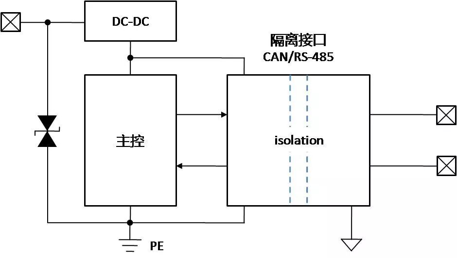
Figure 1
Next, we will analyze:
-
Assuming sufficient protective measures are in place on the control side, when the control side interface experiences electrostatic discharge, the energy is released to PE through the control side protector, having little effect on the isolated communication interface, as shown in Figure 2.
-
When the bus interface experiences electrostatic discharge, due to the bus side being floating, the energy can only be released through the equivalent capacitance Ciso of the isolation barrier. Since Ciso is very small, only a few picofarads to a dozen picofarads, it charges rapidly, and the voltage Viso across it becomes very high, almost equal to the discharge voltage. This voltage is entirely applied to the isolation barrier module’s isolation barrier, and if the voltage exceeds the isolation barrier’s voltage tolerance, it can lead to damage to the internal isolation barrier, as shown in Figure 3.
Note: For general isolation interface modules, the isolation barrier can only withstand an electrostatic discharge voltage of 4kV, which is very fragile against higher levels of 6kV or 8kV electrostatic discharge, making damage likely.
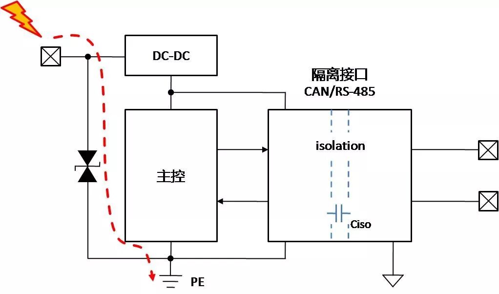
Figure 2
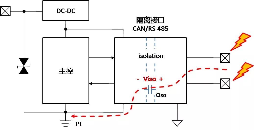
Figure 3
2. Device Control Side Floating
In this state, the device control side reference ground is floating and has no connection to PE, while the bus side is connected to the protective ground (PE), as shown in Figure 4.
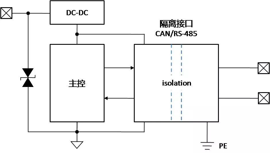
Figure 4
Next, we will analyze:
-
When the bus side interface experiences electrostatic discharge, the electrostatic energy is released through the internal bus side device of the isolation interface module to PE. However, if the ESD energy exceeds the ESD immunity of the internal bus side device of the interface module, the bus interface may be damaged, as shown in Figure 5.
-
When the control side interface experiences electrostatic discharge, due to the control side being floating, the energy can only be released through the equivalent capacitance Ciso of the isolation barrier. Since Ciso is very small, the voltage Viso becomes very high, and this voltage is entirely applied to the isolation barrier of the isolation interface module. If the voltage exceeds the isolation barrier’s voltage tolerance, it can lead to damage to the internal isolation barrier, as shown in Figure 6.
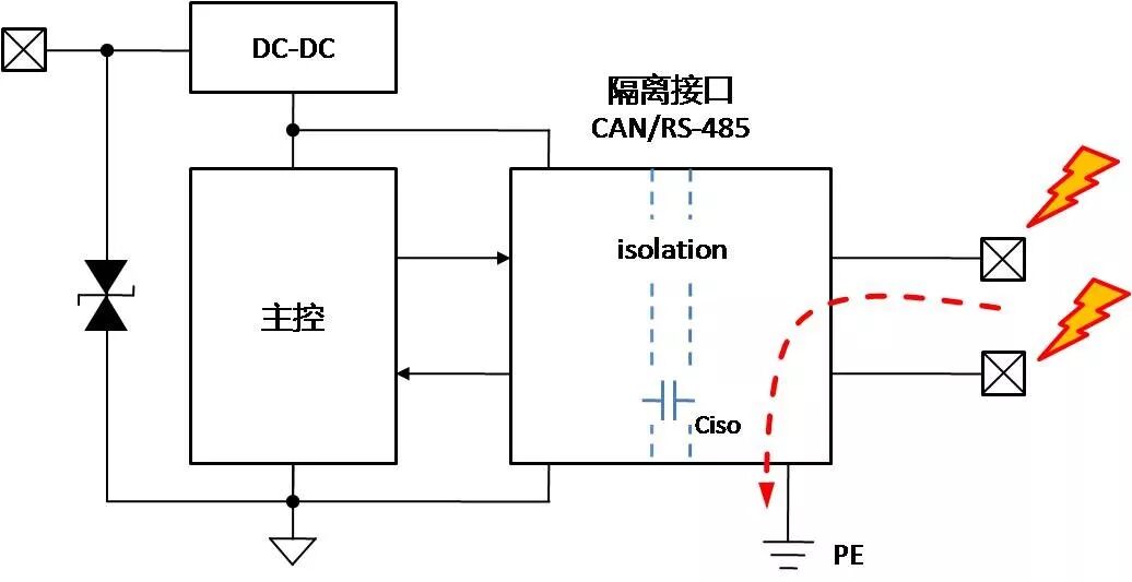
Figure 5
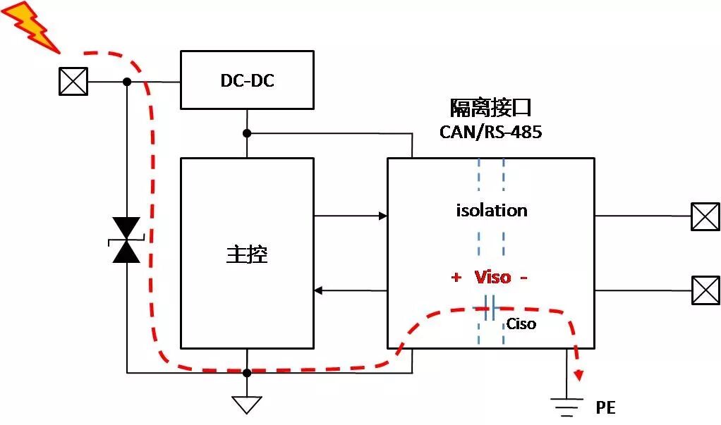
Figure 6
3. Improvement Measures
For the above two situations, the isolation interface module needs effective electrostatic protection. It is recommended to add Cp, Rp, and TVS when designing the isolation interface to enhance the ESD immunity of the isolation interface.
-
The role of capacitor Cp: To reduce the pressure on the isolation barrier, providing a low-impedance path for electrostatic energy. Most of the electrostatic energy is released through this capacitor. To achieve good results, the capacitance value of Cp should be much larger than Ciso, and it is recommended to take between 100pF and 1000pF.
-
The role of the TVS diode: For electrostatic discharge on the bus side, the electrostatic energy will be released through the protective device. Note: Its breakdown voltage must be less than the maximum voltage that the isolation interface can withstand, while being greater than the signal voltage; In high communication rates or with many nodes, it is also necessary to choose devices with small equivalent capacitance to avoid affecting normal bus communication.
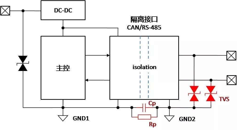
Figure 7
Note: If the product has no safety regulations, a large value discharge resistor, such as 1M, can be connected in parallel with Cp to prevent static charge accumulation; If there are safety regulations, it is generally necessary to remove the discharge resistor and choose safety capacitors.
Complete Bus Interface Protection Circuit
The previous analysis only covered the mechanism of ESD, but as industrial products increasingly require higher EMC levels for communication interfaces, many applications require compliance with IEC61000-4-2 electrostatic discharge level 4 and IEC61000-4-5 surge immunity level 4. Generally, the ESD and surge protection levels of common transceivers are relatively low, such as the CTM1051M isolated CAN transceiver, which has an isolation voltage of 2500VDC, and under bare conditions, the ESD and surge levels are low. Therefore, it is necessary to add peripheral circuits to improve the EMC level of the communication port.
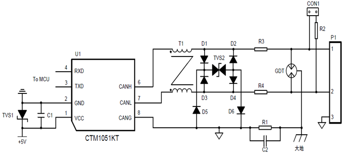
Figure 8
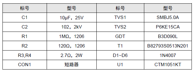
Taking the CAN bus as an example, the above figure shows a recommended complete peripheral circuit. The GDT is placed at the front end, providing primary protection. When lightning or surges occur, the GDT instantly reaches a low-resistance state, providing a discharge path for instantaneous large currents, clamping the voltage between CAN_H and CAN_L to around twenty volts. The actual values can be adjusted based on protection levels and component costs, with R3 and R4 recommended to be PTCs, and D1~D6 recommended to be fast recovery diodes, as shown in the parameter table below.
Table 1 Recommended Parameter Table
Another solution is to use ZLG’s SP00S12 surge protection module, which can be used for various signal transmission systems to suppress harmful signals such as lightning, surges, and overvoltage, protecting the device’s signal ports. When paired with ZLG’s fully isolated CTM or SC series isolated CAN transceivers, as shown in the figure below, it can greatly enhance the product’s integration while significantly shortening the development cycle.
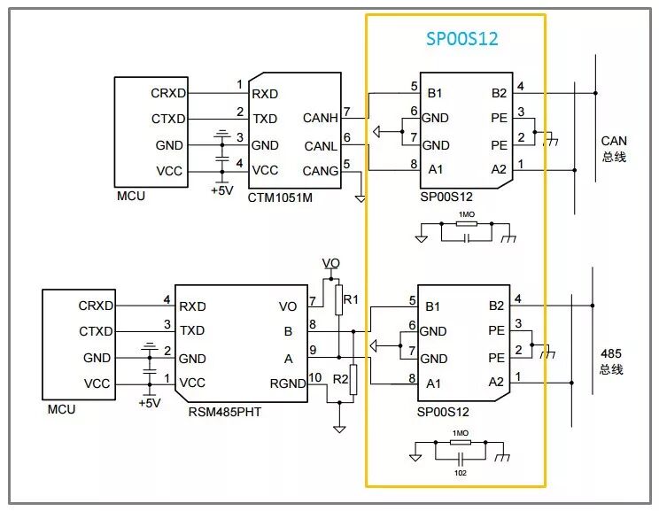
Figure 9
The Necessity of Grounding the RC Circuit
The previous sections discussed the principles of grounding after bus isolation and recommended circuits. Many customers in the field often ask why RC grounding is necessary after bus isolation. Here is a brief description:
1. Capacitor: From the perspective of EMS (Electromagnetic Susceptibility), this capacitor is intended to reduce potential impacts (the influence of high-frequency interference signals on the circuit, referenced to ground level) under the assumption that PE is well connected to the ground. It is meant to suppress the transient common-mode voltage difference between the circuit and the interference source. Ideally, GND should be directly connected to PE, but direct connection may be impractical or unsafe. From the EMI (Electromagnetic Interference) perspective, if there is a metal shell connected to PE, this high-frequency path can also prevent high-frequency signals from radiating out.
2. 1M Resistor: This is used to deal with ESD (Electrostatic Discharge) testing. In systems where the capacitor connects PE and GND (floating systems), during ESD testing, the charge injected into the tested circuit has no place to discharge, leading to gradual accumulation, raising or lowering the GND level relative to PE. Once the accumulation exceeds the voltage tolerance of the weakest insulation point between PE and the circuit, a discharge occurs between GND and PE, generating tens to hundreds of amperes of current on the PCB in a few nanoseconds, which is sufficient to cause any circuit to fail due to EMP (Electromagnetic Pulse) or damage the weakest insulation point in the signal connection device between PE and the circuit. However, if direct connection between PE and GND is not possible, a 1~2M resistor can be used to slowly release this charge, eliminating the pressure difference between the two. Of course, the 1~2M value is chosen based on ESD testing standards, as IEC61000 specifies a maximum repetition rate of only 10 times/second. If you conduct a non-standard ESD discharge at 1000 times/second, I believe that a 1~2M resistor will not be able to release the accumulated charge.
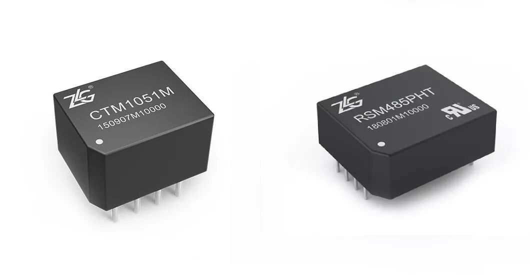
ZLG provides high-quality and reliable isolated CAN transceivers and isolated RS-485 transceivers, with full isolation of power and signals, isolation voltage up to 3500VDC and above, ensuring the safety of your CAN and RS-485 buses!

If you have any questions, you can:
 Add WeChat: zlgmcu-888
Call ZLG’s official technical hotline: 400-888-4005.