This morning, Huawei HiSilicon officially released the Kirin 950, with detailed performance introduced later in the article. This article also takes the opportunity to review the development process of HiSilicon and how the Kirin 950 was forged. Interested friends can join the discussion.
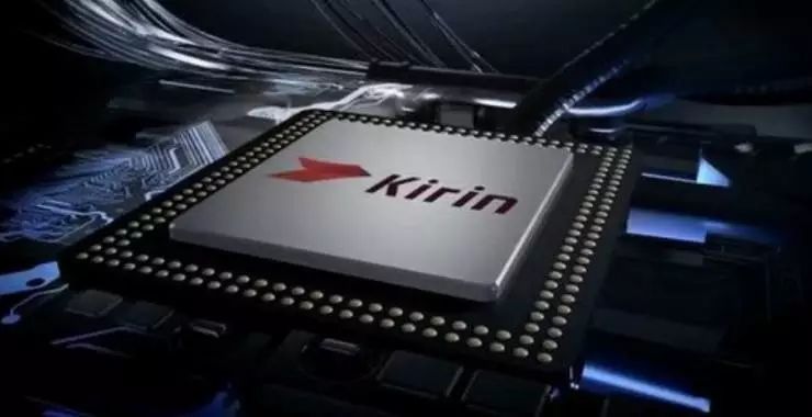
HiSilicon Semiconductor Co., Ltd. is a wholly-owned subsidiary of Huawei and ranks first among domestic IC design companies in terms of operating revenue. The company was established in October 2004, originally as Huawei’s Integrated Circuit Design Center.
HiSilicon has a wide range of products, including fixed and wireless networks, network access terminals, and wireless terminals, which are widely used in Huawei’s optical communication and data communication products, including router chips, set-top box chips, mobile tablet chips, video surveillance chips, switch chips, and photonic chips. In the video surveillance chip field, HiSilicon is almost dominant in China.
Since the main character of this article is the HiSilicon Kirin, other chips are automatically filtered, and only the most well-known HiSilicon mobile chip – Kirin – is discussed.
Development Route of Kirin
At the recently held 2015 China Computer Conference, Academician Li Guojie of the Chinese Academy of Engineering spoke about the gradual formation of three routes for the development of domestic CPUs:
One is the independent design route, independently constructing the basic software and hardware system, represented by Loongson and Shenwei;
One is the ARM technology route, purchasing ARM instruction authorization or hard/soft core authorization, represented by HiSilicon and Spreadtrum;
And the last is the ODM route, cooperating with foreign companies, entrusting foreign designs, and obtaining partial product ownership, represented by Zhaoxin and Hongxin.
So, why did Huawei HiSilicon choose the ARM route? This needs to start from the reasons and purposes of Huawei HiSilicon’s development of mobile chips.
Reasons and Purposes for Huawei’s Development of Mobile Chips:
On one hand, the original partner Texas Instruments might gradually withdraw from the mobile chip market – being pushed out by Qualcomm’s communication patents and the practice of buying basebands with SoCs;
On the other hand, it is also to enhance the self-sufficiency capability of core components, avoiding being exploited by suppliers.
If an independent route is chosen, it would be extremely difficult to recover from the market. Therefore, it is only natural to choose the development route of purchasing ARM’s IP cores to integrate into SoCs – purchasing ready-made IP cores (ARM), GPU cores (GC, Mali), and various interface IP cores (Synopsys), and through a certain process, integrating them into SoCs.
Although choosing the ARM technology route has a more commercialized scent, it lacks the ideal belief of solving industrial development and information security issues. However, relying on the AA system greatly reduces the R&D financial cost, time cost, and technical threshold, which is very beneficial for achieving market-oriented operations.
The Tragic K3
The growth of Kirin has also been a journey of setbacks and growth through trials.
From 2009 to 2010, HiSilicon developed and promoted its first mobile SoC – Hi3611 (K3), which integrated a dual-core ARM-11 and was used in smartphones and other smart devices.
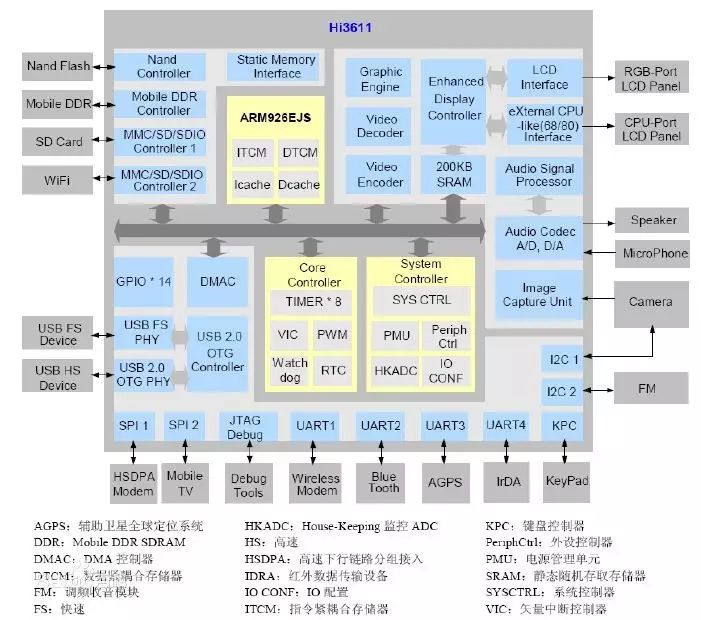
Although Huawei had high hopes for K3, the reality was harsh – K3 ultimately could not even establish itself in the counterfeit phone market.
Why is that? On one hand, there are indeed issues with K3 itself. But more importantly, it lacked strong partners and had problems with market positioning and marketing.
Since the mobile chip market was basically occupied by Texas Instruments, Qualcomm, MediaTek, and other manufacturers, K3 could only compete for the lowest-end counterfeit market, where counterfeit manufacturers had limited technical strength and quality control could not be compared with major manufacturers. Many issues were actually caused by the counterfeit manufacturers themselves, but were ultimately attributed to the K3 product’s shortcomings.
Additionally, the development of any entity follows a spiral process, which must go through the steps of discovering problems, analyzing problems, and solving problems. For instance, MediaTek, which entered the mobile chip market in 2004, leveraged TCL’s mobile solution company, Jiekai Communication, to solve bugs and improve chips.
Similarly, K3 could not be an exception. Because counterfeit manufacturers had poor technical strength, they could not provide feedback on existing issues during use, which would lead to joint improvements on the chip. Instead, due to the large shipment volume, they tarnished K3’s reputation.
Finally, the marketing approach was also highly questionable. Without choosing to develop 1 to 2 strong clients while the product was immature, it instead developed over a dozen small clients and heavily distributed products, causing significant management difficulties and ultimately leading to substantial inventory accumulation among distributors…
Thus, K3’s fate was tragically sealed, but this was far from the end of the Kirin chip tragedy.
The Pitiful K3V2
In January 2012, HiSilicon released K3V2, which integrated a quad-core ARM A9 and chose the GC4000 from Imagination Technologies for GPU. Due to the inability to secure TSMC’s latest 28nm process technology, it had to settle for the 40nm process, which laid the groundwork for K3V2’s shortcomings.
In terms of application processors, in 2012, HiSilicon’s design experience was not competitive even when compared to domestic manufacturers like Allwinner and Rockchip, let alone international giants like Texas Instruments and Qualcomm. As the first released quad-core A9 SoC, HiSilicon clearly could not position the product as “high-end” as advertised.
For the GPU, the choice of GC4000 was another misstep. Although GC4000 has a good theoretical performance/chip area ratio and smaller chip area, leading to relatively lower costs, its performance relied heavily on frequency increases.
Due to the choice of the 40nm process, it directly resulted in higher power consumption, and many Huawei mid-to-high-end phones equipped with K3V2 were jokingly referred to as “hand warmers.” To control power consumption, HiSilicon had to reduce the frequency of GC4000 from the originally intended 600MHz to 480MHz, and in some applications, the GPU frequency was even capped at a maximum of 240MHz.
As previously mentioned, to control power consumption, HiSilicon reduced the GPU frequency significantly, leading to poor gaming experiences with K3V2 – many major games had frequent compatibility issues, some had black screens, and some exhibited texture errors; even minor games faced issues with insufficient smoothness.
Thus, high heat generation, poor gaming experience, and numerous small issues became synonymous with K3V2. To support the Kirin chip, Huawei suppressed dissenting voices from Huawei’s terminal company and insisted on using K3V2 in its mid-to-high-end models for two years. Specifically, from 2012 to 2014, models like P2, D2, Mate1, P6, Honor 2, and Honor 3 were successively launched.
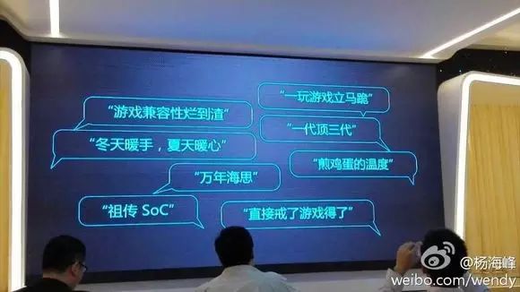
(Huawei’s self-deprecating remark about K3V2)
To be honest, K3V2 is a huge pit, which indeed put Huawei, its “parent,” in a difficult position – it completely lost to the Snapdragon 600 and other SoCs used in Xiaomi phones in terms of performance, power consumption, compatibility, and stability, significantly affecting the sales of Huawei’s mid-to-high-end models. Many fans who were disappointed by K3V2 turned against Huawei, avoiding phones equipped with HiSilicon chips.
Some say that the Kirin chip is not sold externally for differentiation competition. While this is true, it also requires someone to be willing to buy it. The K3V2 of that year was completely uncompetitive in the market.
It can be said that if it weren’t for Huawei’s coordination among its subsidiaries in a way that embodies the characteristics of a planned economy, and if it hadn’t adopted a vertically integrated model to provide comprehensive support for HiSilicon in terms of funding, deployment platforms, and sales channels, the Kirin chip would have long been drowned in the fierce tide of market competition after experiencing the failures of K3 and K3V2.
Getting Back on Track: Kirin 910, 92X, 93X
As the saying goes, “One learns from failure.” After experiencing two defeats, HiSilicon accumulated experience and learned lessons. In 2014, HiSilicon made significant modifications to K3V2 – upgrading the 40nm process to 28nm and replacing the GC4000 with Mali450MP4, successfully solving compatibility and power consumption issues, thus creating HiSilicon’s first usable SoC – Kirin 910.
In May 2014, a usable SoC was released – Kirin 920, which consisted of a quad-core A7, a quad-core A15, and Mali628MP4, achieving a good balance between performance and power consumption, and compatibility was also improved due to the use of Mali’s GPU, correcting the public’s impression of HiSilicon chips being power-hungry, incompatible, and having many small issues.
The highlight of the Kirin 92X series chips was not the CPU and GPU, as these were essentially purchased foreign technologies and products. The real highlight was Huawei’s self-developed communication module (baseband). Huawei has a deep foundation in communication technology, and the Balong 720 baseband of the 920 supports five standards: TD-LTE/LTE FDD/TD-SCDMA/WCDMA/GSM (which means it supports 2G/3G/4G for China Mobile and Unicom and 4G for China Telecom), making it the world’s first commercial LTE Cat6 chip solution.
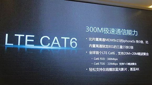
How important is the baseband? The ability to make calls, send messages, and access the internet on a mobile phone largely depends on the baseband’s role. The former leader, Texas Instruments, had to exit the mobile chip market due to baseband issues, and giants like Intel and NVIDIA have struggled in the mobile chip market due to their reliance on baseband technology and software ecosystem factors.
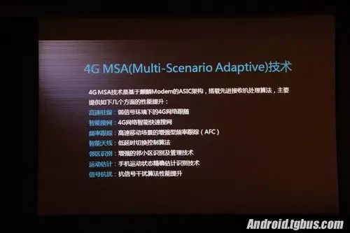
The AP of the Kirin 93X series chips integrates an 8-core A53 and Mali628MP4, with limited performance improvements, achieving a relatively balanced performance and power consumption; according to enthusiasts’ tests, the single-core A53 power consumption is about 500mW. The highlight of the 93X series chips is also the baseband, which alleviates signal instability or poor signals in high-speed mobile scenarios and underground environments.
Leap Forward: Kirin 950
On November 5, Huawei HiSilicon released the Kirin 950, which integrated four ARM Cortex A53 and four ARM Cortex A72 cores. The official claim states, “A72 improves performance by 11% over A57 while reducing power consumption by 20%.”
For the GPU, it used Mali T880MP4, with the official claim of “100% improvement in graphics generation capability and GFLOPS over the previous generation GPU.” Although there is no direct 1VS1 comparison, according to ARM’s data, the performance of Mali T760MP8 is likely to be stronger than that of Mali T880MP4. The GPU of Kirin 950 may not outperform Samsung’s Exynos 7420 released last year – Huawei adheres to the philosophy of “good enough” and has been “stingy” with GPUs.
In the on-site benchmark demonstration, the Kirin 950 scored a high of 82,220 in AnTuTu v5.6.2, compared to Samsung’s Exynos 7420, which scored over 70,000. Considering the comparison between Exynos 7420 and Kirin 950 in terms of GPU performance, the A72 shows a certain degree of improvement over A57. (This benchmark was conducted on a bare development board and results may differ when tested on a phone.)
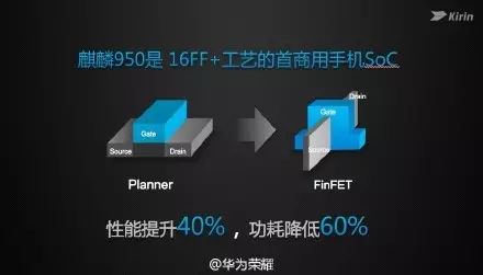
In terms of process technology, it adopts the industry’s leading TSMC 16nm FF+ process and is the first commercial SoC chip using 16nm FF+ technology. This is distinguished from Apple’s TSMC A9, which uses 16nm FF+ process, as A9 uses Qualcomm’s external baseband, and strictly speaking, can only be considered an AP, not an SoC.
Compared to 28nm HPM, the official claim is, “Performance improves by 40%, while saving 60% of power consumption.”
Although it cannot yet be proven by physical testing, referencing the 14nm process of Exynos 7420, which did not exhibit the overheating issues seen in Snapdragon 810, and considering HiSilicon’s good performance in power control – Kirin 910, Kirin 920, and Kirin 930 all achieved a good balance between power consumption and performance. The Kirin 950, using the 16nm FF+ process, should not become a “heating” SoC.
In terms of coprocessors, the Kirin 950’s I5 coprocessor can relieve the main processor, improving the phone’s battery life.
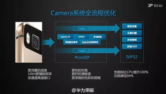
In terms of photography, the Kirin 950 resets the camera system, supporting 14-bit dual ISP, with throughput performance improved by 4 times, reaching up to 960MPixel/s; it supports hybrid focusing technology, which adapts to choose the best focusing method according to the shooting scene; in addition, there are more filter effects to experience interesting photography.
In terms of radio frequency chips, the Kirin 950 adopts a new self-developed RF chip that not only has a higher integration but also lower power consumption, supporting a wider frequency range (450MHz – 3.5GHz), allowing the phone to support a broader range of global roaming.
Additionally, the Kirin 950 adopts new LPDDR4 and new system buses, strengthening hardware performance. The Kirin 950 also optimizes chip boost performance and sustained performance of the chip system, ensuring that user-triggered operations respond within 100 milliseconds; under normal working conditions, it ensures that each frame of drawing is completed within 1/60 of a second.
Conclusion
Indeed, the development model of HiSilicon relying on the AA system cannot construct an independent technology system belonging to China, and its significance for achieving autonomous control over basic software and hardware is limited, nor can it solve the predicament of China’s integrated circuit industry being constrained by others and national information security being compromised. However, its commercial success has indeed reclaimed part of the market from international giants like Qualcomm, and its independent innovation in baseband technology is worthy of respect from the Chinese people.
The success of HiSilicon Kirin stems from Huawei’s significant investments in HiSilicon, the technology system created by ARM and Google, Huawei’s vertical integration model, and the hard work of Huawei employees.
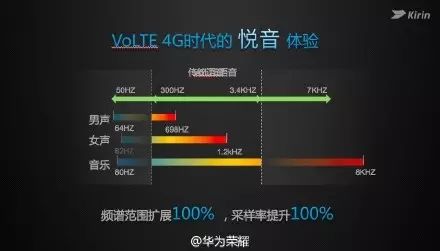
It is understood that China Mobile will fully commercialize VoLTE by the end of 2015, and the entire series of Kirin 920/930/950 chips supports VoLTE. Industry insiders point out that this will bring users a new generation of HD voice experience, significantly shortening call connection delays, and improving video call quality by ten times compared to 3G, while meeting users’ needs for simultaneous calls and internet access.
As the 950 is about to be launched, we wish Kirin good luck.
 Click“Read the original article” to apply fortrial use of “Wago Security Phone” for a total of 10 units, successful applicants will receive it for free