Skip to content
Long press the image to scan and apply for free
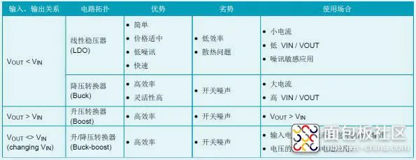
Power management converts various power inputs into output voltages that meet system requirements through specific circuit topologies. The power directly affects system performance, and the key component determining power performance is the Power Management IC (PMIC). It is crucial to understand the selection criteria for PMICs. Understand the Power Usage Environment
To select the appropriate power management component, one must first understand the application environment conditions, such as the system’s input and output parameters. Considerations include:
Is the power input AC or DC? For direct power, is it USB powered or battery powered? Is the input voltage higher or lower than the required output voltage? What is the required load current? Is the load sensitive to noise, or does it require constant current (such as in LED applications), or does it experience significant current variations? Installation space? Achieving greater power in a smaller space.
Different applications have their specific requirements, necessitating corresponding power conversion schemes and matching power management ICs. Common ICs include Low Dropout Regulators (LDOs) and DC/DC switch converters. Among them, DC/DC switch converters include Buck converters, Boost converters, and Buck-Boost converters.
In circuit design, the first consideration is the voltage difference between input and output (VIN – VOUT). Next, based on the specific application requirements, such as efficiency, thermal limitations, noise, complexity, and cost, select the most suitable power management IC.
When VOUT is less than VIN, there is an optionWhen VOUT is less than VIN, the required output current and the VIN / VOUT ratio are important factors in choosing between LDO or Buck. (1) Choose LDO for low VIN / VOUT applications LDOs (Low Dropout Linear Regulators) control the conduction of the switch element in a linear manner to adjust the output voltage, providing accurate and noise-free output voltage, and can quickly respond to load changes at the output. Therefore, they are very suitable for applications requiring low noise, low current, and low VIN / VOUT ratios. When selecting an LDO, consider the range of input and output voltages, the current size of the LDO, and the thermal capability of the package. The dropout voltage of an LDO refers to the minimum voltage of VIN – VOUT within the adjustable range. In low-power applications, such as those powered by a single battery for many years, the LDO’s quiescent current (IQ) must be low to reduce unnecessary battery consumption; such applications require special low-dropout linear regulators (LDOs) with low IQ. However, linear regulation means that the power consumed by the linear regulator’s switch element is the product of the voltage difference and the average load current. A high VIN / VOUT ratio and high load current can lead to excessive power loss. High power-consuming LDOs require larger package sizes, which increases costs, PCB space, and thermal dissipation.
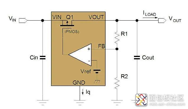 LDO Basic Circuit Schematic
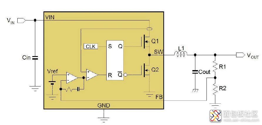
When the LDO power consumption exceeds ~0.8W, a wiser approach is to switch to a Buck converter as an alternative. (2) Choose Buck Converter when VIN / VOUT is high The Buck converter is a type of switching step-down converter that provides high efficiency and high flexibility output under high VIN / VOUT ratios and high load currents. Due to its wide applications, the Buck converter is also known as a step-down regulator or DC-DC step-down switching regulator, and all three essentially refer to the same product. Most Buck converters contain an internal high-side MOSFET and a low-side MOSFET as a synchronous rectifier, controlling the alternating ON/OFF states through an internal duty cycle control circuit to regulate the average output voltage. Noise generated from switching can be filtered by external LC filters.
Buck Converter Basic Circuit Schematic
Since the two MOSFETs switch alternately (ON or OFF), power consumption is very low. By controlling the duty cycle, a large VIN / VOUT ratio output can be generated. The RDS(ON) of the internal MOSFET determines the current handling capability of the Buck converter, while the rated voltage of the MOSFET determines the maximum input voltage. The switching frequency, along with external LC filter components, determines the output ripple voltage; Buck converters with higher switching frequencies can use smaller filter components, but the power loss from switching will increase. Buck converters with Pulse Skipping Mode (PSM) reduce their switching frequency under light load conditions, thus improving efficiency during light load, which is crucial for applications requiring low power standby modes. Some specialized Buck architectures, such as ACOT, have very fast loop responses, making them ideal for power applications requiring very fast load transient responses, such as DDR, Core SoC, FPGA, and SIC.
When VOUT is higher than VIN, choose a Boost Converter
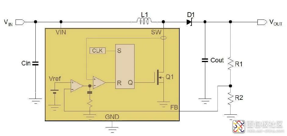
Boost converters are used when VOUT is higher than VIN, allowing the input voltage to be increased to a higher output voltage. Its operating principle involves charging an inductor through an internal MOSFET, and when the MOSFET is turned off, discharging the inductor through a rectifier to the load. The charging and discharging of the inductor results in a reverse voltage, thereby increasing the output voltage above VIN.
Typical boost converter circuits include: an inductor, power MOSFET, rectifying diode, control IC, and input and output capacitors. Common improved configurations generally use two MOSFETs, where the second MOSFET replaces the rectifying diode, turning on when the power switch is off. MOSFETs have lower voltage drops, significantly reducing power loss while improving the efficiency of the regulator.
The ON/OFF duty cycle of the MOSFET switch will determine the boost ratio VOUT / VIN, and the feedback loop also controls the duty cycle to maintain a stable output voltage. The output capacitor acts as a buffer to reduce output voltage ripple. The absolute maximum rating of the MOSFET current and the boost ratio together determine the maximum load current, while the absolute maximum rating of the MOSFET voltage determines the maximum output voltage. Some boost converters integrate the rectifier with the MOSFET internally, achieving synchronous rectification.
Boost Converter Basic Circuit Schematic
When the input voltage is uncertain, choose a Buck-Boost Converter. The Buck-Boost converter is used in applications where the input voltage may change, being either below or above the output voltage. When VIN is higher than VOUT, the four internal MOSFET switches will automatically configure as a Buck converter, while when VIN is lower than VOUT, it switches to Boost operation mode. This makes the Buck-Boost converter very suitable for battery-powered applications, especially when the battery voltage is below the regulated output voltage, extending battery life. Because the four-switch Buck-Boost converter operates in a fully synchronous mode, it can achieve higher efficiency. The output current capability in Buck mode is higher than in Boost mode; because under the same load conditions, Boost mode requires higher switching current. The absolute maximum rating of the MOSFET voltage will determine the maximum input and output voltage ranges. In applications where the output voltage does not need to reference ground, such as LED drivers, a Buck-Boost converter with only a single switch and rectifier can be used. In most cases, the output voltage references VIN.
LDO Basic Circuit Schematic
When the LDO power consumption exceeds ~0.8W, a wiser approach is to switch to a Buck converter as an alternative. (2) Choose Buck Converter when VIN / VOUT is high The Buck converter is a type of switching step-down converter that provides high efficiency and high flexibility output under high VIN / VOUT ratios and high load currents. Due to its wide applications, the Buck converter is also known as a step-down regulator or DC-DC step-down switching regulator, and all three essentially refer to the same product. Most Buck converters contain an internal high-side MOSFET and a low-side MOSFET as a synchronous rectifier, controlling the alternating ON/OFF states through an internal duty cycle control circuit to regulate the average output voltage. Noise generated from switching can be filtered by external LC filters.
Buck Converter Basic Circuit Schematic
Since the two MOSFETs switch alternately (ON or OFF), power consumption is very low. By controlling the duty cycle, a large VIN / VOUT ratio output can be generated. The RDS(ON) of the internal MOSFET determines the current handling capability of the Buck converter, while the rated voltage of the MOSFET determines the maximum input voltage. The switching frequency, along with external LC filter components, determines the output ripple voltage; Buck converters with higher switching frequencies can use smaller filter components, but the power loss from switching will increase. Buck converters with Pulse Skipping Mode (PSM) reduce their switching frequency under light load conditions, thus improving efficiency during light load, which is crucial for applications requiring low power standby modes. Some specialized Buck architectures, such as ACOT, have very fast loop responses, making them ideal for power applications requiring very fast load transient responses, such as DDR, Core SoC, FPGA, and SIC.
When VOUT is higher than VIN, choose a Boost Converter
Boost converters are used when VOUT is higher than VIN, allowing the input voltage to be increased to a higher output voltage. Its operating principle involves charging an inductor through an internal MOSFET, and when the MOSFET is turned off, discharging the inductor through a rectifier to the load. The charging and discharging of the inductor results in a reverse voltage, thereby increasing the output voltage above VIN.
Typical boost converter circuits include: an inductor, power MOSFET, rectifying diode, control IC, and input and output capacitors. Common improved configurations generally use two MOSFETs, where the second MOSFET replaces the rectifying diode, turning on when the power switch is off. MOSFETs have lower voltage drops, significantly reducing power loss while improving the efficiency of the regulator.
The ON/OFF duty cycle of the MOSFET switch will determine the boost ratio VOUT / VIN, and the feedback loop also controls the duty cycle to maintain a stable output voltage. The output capacitor acts as a buffer to reduce output voltage ripple. The absolute maximum rating of the MOSFET current and the boost ratio together determine the maximum load current, while the absolute maximum rating of the MOSFET voltage determines the maximum output voltage. Some boost converters integrate the rectifier with the MOSFET internally, achieving synchronous rectification.
Boost Converter Basic Circuit Schematic
When the input voltage is uncertain, choose a Buck-Boost Converter. The Buck-Boost converter is used in applications where the input voltage may change, being either below or above the output voltage. When VIN is higher than VOUT, the four internal MOSFET switches will automatically configure as a Buck converter, while when VIN is lower than VOUT, it switches to Boost operation mode. This makes the Buck-Boost converter very suitable for battery-powered applications, especially when the battery voltage is below the regulated output voltage, extending battery life. Because the four-switch Buck-Boost converter operates in a fully synchronous mode, it can achieve higher efficiency. The output current capability in Buck mode is higher than in Boost mode; because under the same load conditions, Boost mode requires higher switching current. The absolute maximum rating of the MOSFET voltage will determine the maximum input and output voltage ranges. In applications where the output voltage does not need to reference ground, such as LED drivers, a Buck-Boost converter with only a single switch and rectifier can be used. In most cases, the output voltage references VIN.
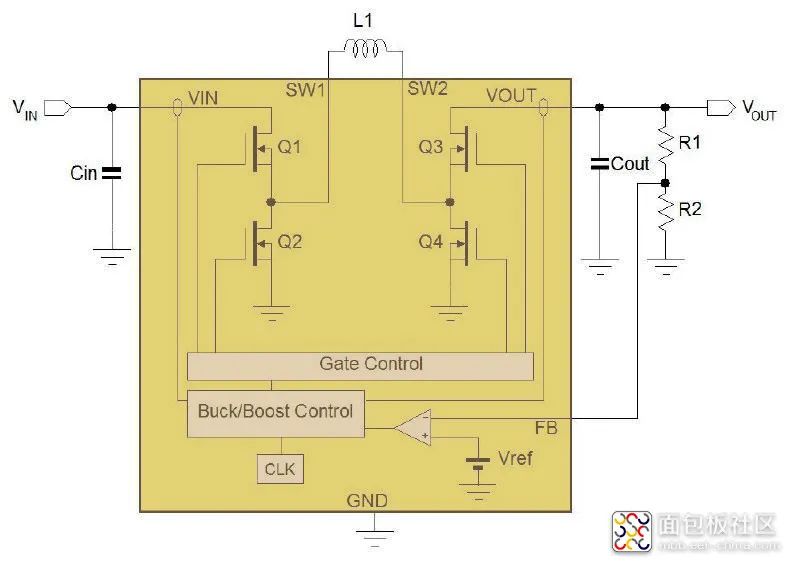 Buck-Boost Converter with Four Internal Switches
Most power management components use one of the four converter architectures mentioned above. For some special applications, such as those requiring very high switching currents (>10A), external MOSFET configurations can be considered. If monitoring power over-voltage or under-voltage conditions is required, dedicated power monitoring ICs can be used.
Author: Hard City Allchips, Source: Breadboard Community
Link: https://mbb.eet-china.com/blog/uid-me-3975615.html
Copyright Notice: This article is original to the author, and reproduction is prohibited without permission!
Buck-Boost Converter with Four Internal Switches
Most power management components use one of the four converter architectures mentioned above. For some special applications, such as those requiring very high switching currents (>10A), external MOSFET configurations can be considered. If monitoring power over-voltage or under-voltage conditions is required, dedicated power monitoring ICs can be used.
Author: Hard City Allchips, Source: Breadboard Community
Link: https://mbb.eet-china.com/blog/uid-me-3975615.html
Copyright Notice: This article is original to the author, and reproduction is prohibited without permission!