Author: Krishna Balachandran, Senior Product Marketing Manager at Synopsys
1
Introduction
Power Management Integrated Circuits (PMICs) are the first circuits to power on in a system and the last to power off. They perform the task of providing the correct voltage to component chips by regulating or boosting voltage levels.
Analog-rich PMICs are particularly susceptible to variations in semiconductor manufacturing. Calibration is a post-manufacturing step that involves determining the relationship between these variations and expected values, as well as canceling or compensating for these variations.
Today’s smart PMICs include programmable power-up and power-down sequences, external event detection, system monitoring for over-voltage and current conditions that could damage the PMIC, fault handling where the PMIC controls the system to prevent power loss, and algorithms for battery capacity prediction and management, all implemented in digital logic. Depending on the end application, some or all functions may need to be activated. Configuration allows for the construction of platform PMICs for a range of applications and enables custom functionalities.
PMICs can be calibrated and configured through Non-Volatile Memory (NVM) to provide the correct voltage and power sequences for target applications or configurable functionalities for end systems.
Some PMICs undergo a single calibration and configuration at the factory, for which a high area-efficient One-Time Programmable (OTP) NVM is the best choice. When a PMIC is expected to be calibrated and reconfigured multiple times during its lifecycle, Multi-Time Programmable (MTP) NVM can be used.
BCD silicon technology combines the advantages of three different process technologies on a single chip: bipolar for precise analog functions, CMOS for digital design, and DMOS for power and high-voltage components. This technology combination brings many advantages to PMICs: higher reliability, reduced electromagnetic interference, and smaller chip area. Due to these advantages, most PMIC manufacturers choose BCD technology for PMIC production.
PMICs can be manufactured in various ways. Due to their sensitivity to cost, PMIC manufacturers typically opt for manufacturing processes with the fewest mask layers. To assist PMIC manufacturers, NVM IP vendors must align with PMIC manufacturers and provide IP across multiple variants of the same process. NVM is highly sensitive to manufacturing processes and must undergo silicon material qualification for the device combinations used by PMIC manufacturers.
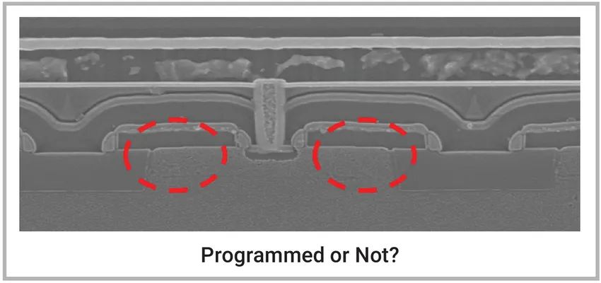
Figure 1: Fuse-based OTP is inherently secure, making it impossible to determine whether the OTP has been programmed
2
The Role of Embedded NVM in PMICs
PMICs are widely used in mobile applications, including smartphones, wearables, hearables, laptops, and tablets. They are also used in smart motor control, lighting control, and industrial control applications.
Today’s PMICs are smart and configurable, built in a modular fashion. Depending on the end application and the required voltage or power sequencing, configurable firmware stored in NVM customizes the PMIC for specific applications. When frequent firmware updates are required in automotive applications, reprogrammable NVM or MTP NVM is the best choice. However, if firmware is expected to be programmed only once during the product’s lifecycle, OTP NVM, which offers higher area efficiency, is preferred.
Additionally, NVM is used to store values for output voltage, current limits, power-up reset delays, power-up delays, voltage ramp rates, standby mode settings, and power good and invalid power condition settings.
Since PMICs contain analog circuits, they require trimming and calibration after manufacturing, either in the factory or in the field, to prepare the product for its intended use. These settings are also stored in embedded NVM.
Why Not Use Wafer-Fabricated Fuses?
Designs at mature process nodes like 350nm and 250nm are simple power management ICs. They are typically analog with minimal digital control logic. Wafer-fabricated fuses are used to store calibration information for analog circuits (up to 2Kb). At small capacities and mature process nodes, wafer-fabricated fuses offer high area efficiency, reliability, and meet their intended use. As PMICs become smarter, introducing more digital control, and as they migrate to more advanced process geometries, larger memory capacities are required.
Fuses do not maintain high area efficiency at larger capacities and are unreliable due to the re-growth issues throughout the product’s lifetime. Fuse re-growth is caused by electromigration, leading to the reconnection of blown fuses, which can change stored values over time. Furthermore, fuses cannot be used to store firmware, which requires 64 – 256Kb of capacity. Lastly, fuses do not provide any security, making the information stored within them visible under a scanning electron microscope, thus making it vulnerable to hacking.
NVM for Advanced Nodes
MTP and fuse-based OTP NVM have been in widespread commercial production for about 10 years, being fully reliable and scalable. Manufacturing NVM devices does not require special masks or process steps. They enter mass production in 180nm and BCD processes with smaller geometries. As BCD processes shrink, MTP and fuse-based OTP have been designed down to advanced nodes of 55nm.
NVM Reliability
In harsh environments for automotive and industrial applications, reliability is another key requirement. MTP and fuse-based OTP NVM have demonstrated exceptional reliability, durability, and data retention capabilities throughout the product’s lifetime, having been properly certified for operating temperatures up to 150°C and even 175°C, and subjected to early failure rate testing.
NVM Security
Fuse-based OTP NVM is not easily affected by any passive or invasive security attacks that attempt to alter voltage or temperature. Since fuse-based OTP NVM operates on the principle of oxide breakdown to represent programmed bits, it is visually indistinguishable between programmed and unprogrammed bits, even with a scanning electron microscope.
MTP and fuse-based OTP NVM designed specifically for PMIC applications provide all-around benefits: cost-effectiveness, lowest power consumption, optimized programming and erase cycle times, and fast read times at system startup.
3
Considerations for Choosing NVM for PMICs
When selecting a foundry for manufacturing, PMIC designers should first consider the following factors:
-
End market (consumer or automotive)
-
Product requirements of the end market
-
Choice of process node (based on prior analysis)
-
Expected production volume
-
Expected wafers needed within a specific timeframe
-
Foundry
-
Ability and willingness to allocate wafers for PMIC manufacturers’ projects
-
Meeting expected wafer pricing.
After making these decisions, PMIC manufacturers begin searching for available and qualified NVM IP in the chosen foundry and process node.
The four most important considerations for selecting NVM IP are:
-
Capacity Availability
With the recent surge in global demand for wafers used in PMICs, foundry capacity is tight, and PMIC design companies are striving to find a semiconductor manufacturing supplier that can provide wafer allocations in a timely manner and at reasonable prices to meet product growth forecasts.
-
Total Cost of Ownership
Total cost of ownership is the sum of IP procurement costs, silicon costs, and NVM programming costs.
-
Security
NVM that stores critical voltage and current values, power sequences, and potential firmware code must be secure and reliable to ensure system safety.
-
Reliability and Durability
NVM for automotive applications must be designed and validated according to the automotive Physical Design Kit (PDK) provided by the foundry and comply with strict automotive design guidelines.
4
DesignWare NVM IP for PMIC Applications
DesignWare® MTP NVM IP and DesignWare OTP NVM IP provide scalable and reliable embedded memory NVM solutions in standard CMOS and BCD processes without additional process or mask steps. Proprietary technology offers smaller silicon footprints and optimizes programming and read access times. The built-in security features of fuse-based OTP NVM prevent active and passive attacks, tampering, hacking, and reverse engineering.
Customizable macros enable design flexibility in PMIC applications that require secure storage of trim, calibration, and configuration information.
DesignWare MTP NVM IP and DesignWare OTP NVM IP meet automotive AEC-Q100 Grade 0 and Grade 1 temperature standards, accelerating SoC-level development, even in harsh automotive manufacturing environments. They are available across multiple foundries and process nodes.
Synopsys’s MTP and fuse-based OTP NVM IP have been widely used in various systems, including the most advanced PMICs in consumer and automotive applications.
5
Conclusion
All systems require careful delivery of voltage and current to components for reliable and predictable functionality. PMICs provide meticulously controlled voltage and current for the normal operation of consumer, automotive, and industrial applications. PMICs are analog-rich designs that require calibration to compensate for and correct variations in semiconductor manufacturing. Newer PMICs incorporate increasing amounts of digital logic, allowing for customization and configuration for multiple end applications. OTP or MTP NVM is the ideal choice for storing calibration and configuration information.
Synopsys DesignWare NVM IP offers OTP and MTP NVM in standard CMOS and BCD process technologies without additional masks or process steps. Synopsys’s MTP and fuse-based OTP NVM IP feature smaller die sizes, with built-in security features that prevent active and passive attacks, tampering, hacking, and reverse engineering. They have been widely applied across various systems, covering highly developed PMICs in consumer and automotive applications.

 Follow Us