
Milestone Breakthrough in Two-Dimensional Semiconductor Chips!
Fudan University National Key Laboratory of Integrated Chips and Systems
Team led by Zhou Peng and Bao Wenzhong
Successfully developed the world’s first
32-bit RISC-V architecture microprocessor
based on two-dimensional semiconductor materials
“Wuji (无极)”


This achievement breaks through the engineering bottleneck of two-dimensional semiconductor electronics
and achieves an integration density of 5900 transistors for the first time.
It is a domestically developed technology
with independent intellectual property rights completed by the Fudan team,
which gives China a first-mover advantage in the development of new generation chip materials
and provides strong support for advancing electronics and computing technology into a new era.
The related results were published on the evening of April 2, Beijing time,
entitled “A RISC-V 32-Bit Microprocessor Based on Two-dimensional Semiconductors” in the journal Nature.

115→5900
Achieving the largest scale verification record for two-dimensional logic chips
Faced with the global challenge of the physical limits of Moore’s Law, two-dimensional semiconductors with a thickness of a single atomic layer are currently recognized as the key to breaking through. Scientists have been exploring how to apply two-dimensional semiconductor materials in integrated circuits.
For more than a decade, the international academic and industrial communities have mastered wafer-level two-dimensional material growth technology, successfully manufacturing high-performance basic devices with hundreds of atomic lengths and several atomic thicknesses. However, before the Fudan team achieved this new breakthrough, the highest integration density of two-dimensional semiconductor digital circuits internationally was only 115 transistors, achieved by a team from the Vienna University of Technology in Austria in 2017.
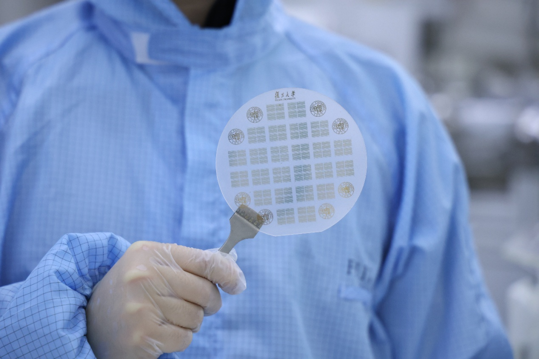
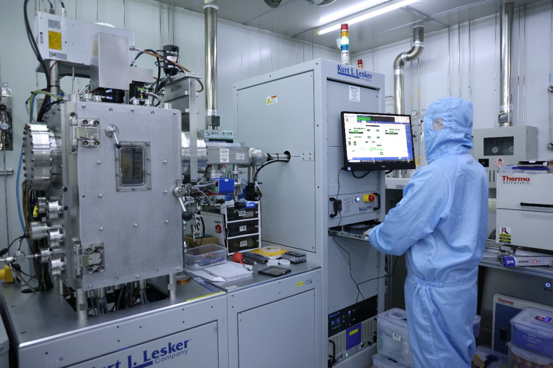
The core challenge lies in assembling these atomic-level precision components into a complete integrated circuit system, which is still constrained by the collaborative yield control of process precision and scale uniformity. After five years of hard work, the Fudan team pushed the chip from array-level or single-tube level to system-level integration, successfully producing the 32-bit RISC-V architecture microprocessor “Wuji (无极)” made from two-dimensional semiconductor materials (MoS2).
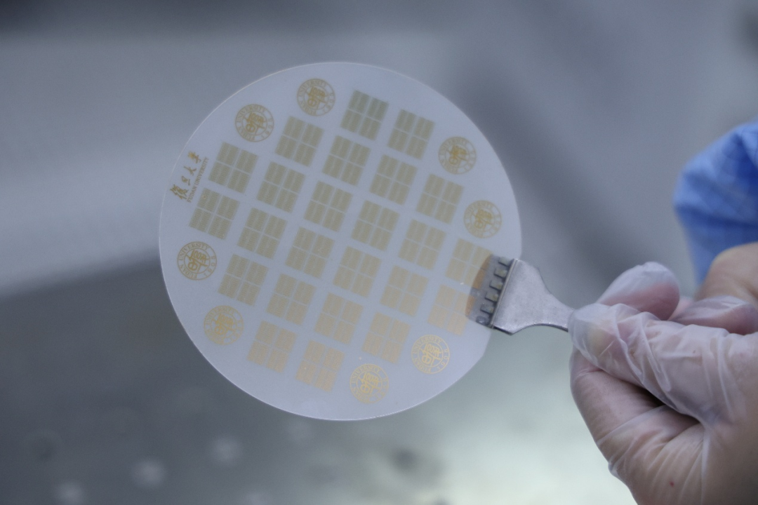
This chip, through innovative integrated processes and the open-source reduced instruction set computing architecture (RISC-V), integrates 5900 transistors, achieving the largest scale verification record for two-dimensional logic chips internationally.
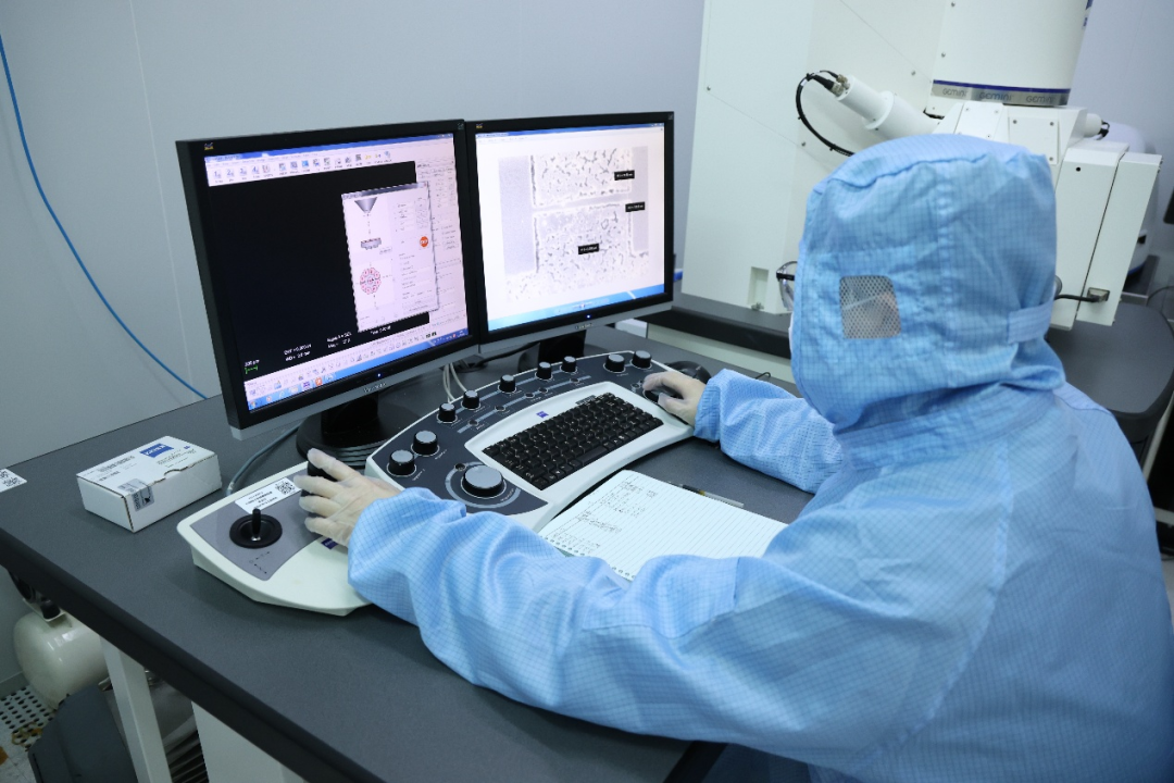
“An inverter is a very basic and important logic circuit, and its yield directly reflects the quality of the entire chip.” Professor Zhou Peng from Fudan University’s School of Microelectronics explained that two-dimensional materials cannot grow high-quality large-size single crystals like silicon wafers through the Czochralski method, but must be grown using chemical vapor deposition (CVD) methods, which leads to defects and non-uniformity in the materials themselves. The inverter yield in this study reached 99.77%, with excellent performance such as single-stage high gain and ultra-low leakage in the off state, marking an engineering breakthrough.
▲
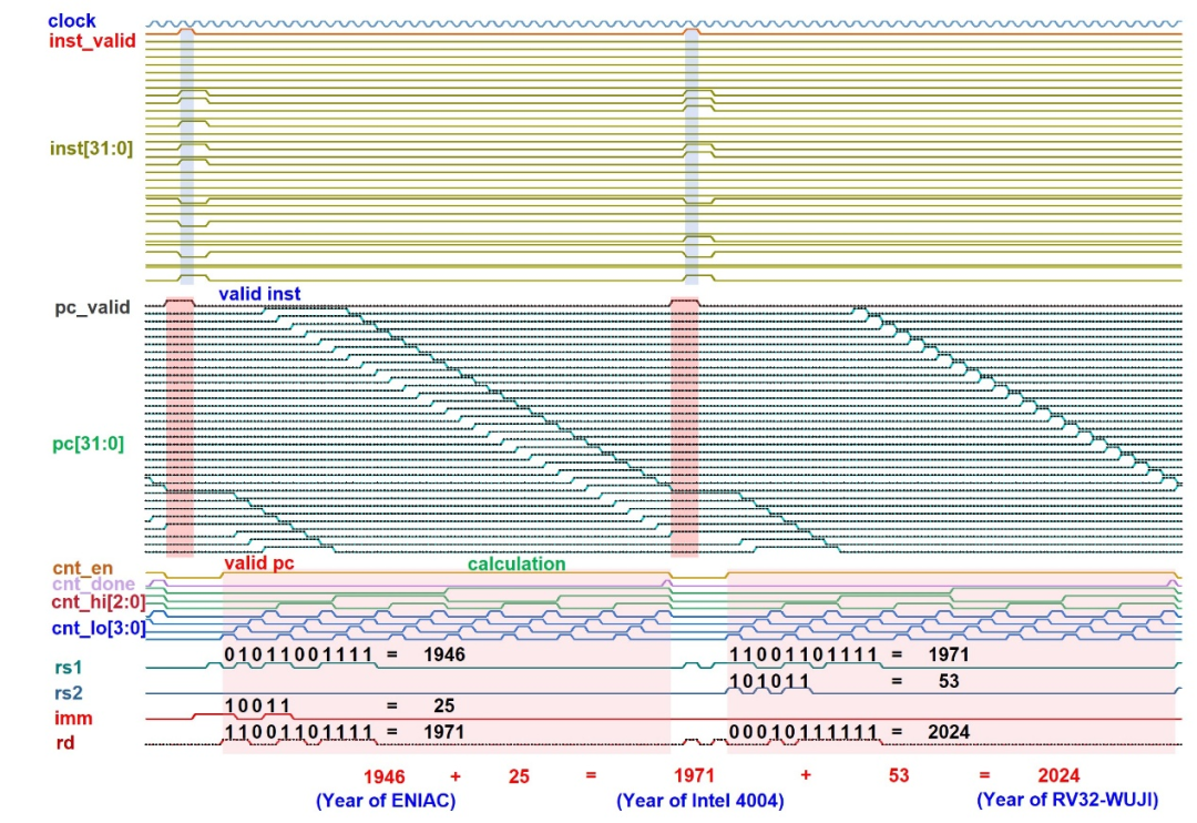
Establishing a computational relationship between ENIAC, Intel 4004, and the year of Wuji’s birth
“We need to ensure that every process can seamlessly connect with other steps to achieve the highest yield and best performance.” Aiming to ensure the highest yield and best performance, the paper’s co-first author and doctoral student from the School of Microelectronics, Ao Mingrui, introduced that the team manufactured 900 inverter arrays, each containing 30×30 inverters. After rigorous testing, it was found that 898 inverters had intact logical functions, with very ideal flip voltage and controversy values, leading in similar research.
“If manufacturing silicon-based chips is like carving on stone, then two-dimensional chips are like carving on tofu.” Researcher Bao Wenzhong from the School of Microelectronics likened that two-dimensional semiconductors, as the thinnest form of semiconductors, must use gentler and more refined process methods for “sculpting.”
The team used low-energy processes such as flexible plasma treatment technology to process the surface of two-dimensional semiconductors, avoiding damage from high-energy particles to the materials, fully leveraging the advantages of two-dimensional semiconductors, and ensuring chip quality.

AI for Science
Efficiently Screening Optimal Process Parameter Combinations
The production of two-dimensional semiconductor chips involves hundreds of processes, with each step affecting the others, leading to astronomical combinations of these process parameter variables. This is also the greatest difficulty in the research and development of two-dimensional semiconductors.
“It is almost impossible to adjust parameters manually.” Bao Wenzhong explained that in the field of two-dimensional semiconductors, the complexity of developing process parameters far exceeds that of traditional silicon-based processes. How can we ensure that each process step can work in synergy with others? Facing this challenge, AI for Science provides a new solution.
As early as 2021, the team published an article in Nature Communications (https://www.nature.com/articles/s41467-021-26230-x) exploring the optimization of process parameters using machine learning methods, and this research is developed based on that foundation. “We accumulated a large amount of process parameters in the early stages, allowing AI to calculate the optimal process formula. Without this prior data accumulation, the effectiveness of AI would be greatly reduced,” Ao Mingrui said.
Through the dual engines of “atomic-level interface precision control + full-process AI algorithm optimization”, the team achieved precise control from material growth to integrated processes, quickly screening the optimal combinations of process parameters, greatly improving experimental efficiency.
For example, in the optimization of the contact layer process, the team collected a large amount of historical data, including variations in contact resistance under different conditions. After inputting this data into the AI model, the AI model could predict the optimal growth parameters and doping concentrations for the contact layer based on existing data under the researchers’ guidance. In subsequent processes, the team also applied AI technology, involving precise coupling control of multiple steps to ensure that each operation achieved the best results.
The resulting product exhibits excellent performance such as single-stage high gain and ultra-low leakage in the off state. Through rigorous automated testing equipment, the team verified that at a 1 kHz clock frequency, the thousand-gate chip could serially implement 37 types of 32-bit RISC-V instructions, meeting the requirements of the 32-bit RISC-V integer instruction set (RV32I). Its integration process optimization level and the verification results of scaled circuits have reached the best level internationally at the same time.
“This indicates that our chip can not only perform simple logical operations but also execute complex instruction sets,” said Zhou Xiucheng, co-first author of the paper and doctoral student from the School of Microelectronics.
Fully Independent R&D
Reaching International Leading Level
RISC-V, as an open-source reduced instruction set computing architecture, has gradually become the mainstream choice in the current chip R&D field. The chip developed this time is based on the RISC-V architecture as its design foundation.
“Our ultimate goal is to bring technology to every household and establish an open and compatible user ecosystem.” Researcher Han Jun from the School of Microelectronics, responsible for RISC-V architecture design in this work, introduced that choosing this architecture means aligning with global technical standards without relying on closed architectures, allowing for the future construction of a user ecosystem that is not constrained by foreign manufacturers’ architectures and IP patents.
In the two-dimensional semiconductor integrated processes developed by the team, about 70% of the processes can directly use existing mature technologies from silicon-based production lines, while the core two-dimensional special processes have constructed a self-owned technology system that includes more than 20 process invention patents, paving the way for industrialization.
Next, the team will further improve the chip integration level, seeking and establishing a stable process platform to lay the foundation for the future development of specific application products. Zhou Peng mentioned that in real-time signal processing, two-dimensional semiconductor chips are expected to be applicable in cutting-edge computing scenarios such as the Internet of Things, edge computing, and AI inference.
Currently, international research on two-dimensional semiconductors is still in its infancy, and large-scale applications have not yet been realized. Against the backdrop of increasingly fierce competition in the global semiconductor field, this achievement signifies that China has the opportunity to gain a leading advantage in two-dimensional semiconductor materials.
“We hope to seize the high ground in this field through continuous technological innovation and application expansion.” Zhou Peng said.
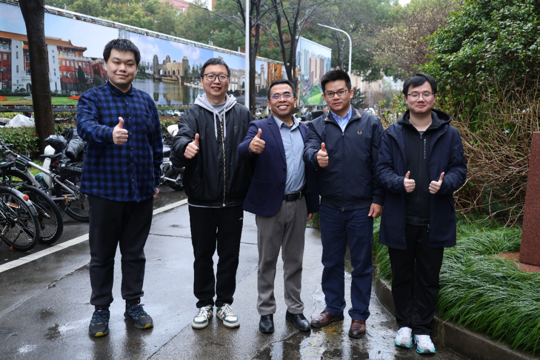
Fudan University National Key Laboratory of Integrated Chips and Systems, Zhejiang Shaoxin Laboratory (Shaoxing Fudan Research Institute), Professors Zhou Peng and Bao Wenzhong from the School of Microelectronics are the corresponding authors of the paper, with doctoral students Ao Mingrui and Zhou Xiucheng as co-first authors. The research work was supported by projects from the Ministry of Science and Technology, the National Natural Science Foundation, the Shanghai Municipal Science and Technology Commission, and the support of the Ministry of Education’s innovation platform.
Paper Link:
https://www.nature.com/articles/s41586-025-08759-9
Source: Fudan University WeChat Official Account