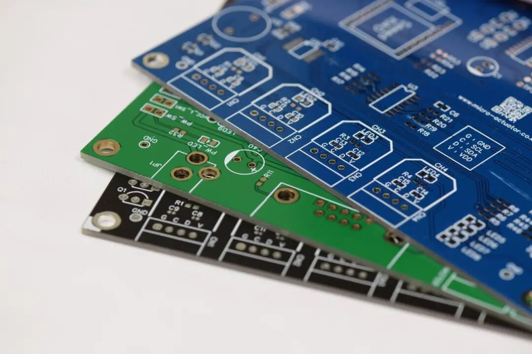
In the production of high multilayer PCBs, the drilling process directly determines the yield and reliability of the product. Industry data shows that the scrap rate of PCBs due to unreasonable hole diameter design can be as high as 30%, with poor hole processing in high multilayer boards accounting for over 45%. This article strictly adheres to the commonly accepted standards in the PCB industry and the process data from leading manufacturers, focusing on the core dimensional requirements, process limitations, and pitfalls to avoid in high multilayer PCB drilling, providing engineers with actionable design specifications.
1
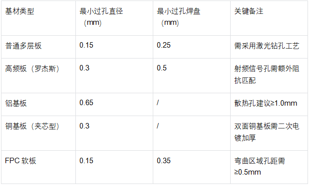
Corresponding Specifications for Substrate Types and Minimum Hole Diameters
The difficulty of drilling high multilayer PCBs increases exponentially with the number of layers, and the physical properties of different substrates directly determine the minimum processable hole diameter. The following data summarizes the processing capabilities of mainstream manufacturers in the industry, with marked sections indicating special requirements for high multilayer boards:
2
Design Restrictions for Slot Holes and Special Holes
The processing of slot holes in high multilayer PCBs is a technical challenge, especially since the dimensional accuracy of metallized slot holes directly affects inter-layer conductivity. According to industry practice data, the following restrictions must be strictly adhered to:
1. Basic Size Requirements for Slot Holes
- Metal slot holes: minimum width 0.5mm (recommended ≥0.65mm for high multilayer boards), processed using a 0.65mm drill bit
-
Non-metal slot holes: minimum width 1.0mm, aluminum/copper substrates must be ≥1.6mm, the diameter of the milling cutter determines the lower limit of slot width
- Short slot restrictions: slots with a length-to-width ratio < 2.5 are prone to drilling defects, and the design must ensure length/width ≥ 2.5
2. Slot Hole Ring Width and Process Matching
The copper ring width (ring width) at the edge of the slot hole is key to preventing solder explosion holes:
-
Recommended ring width > 0.3mm, limit value 0.2mm (only applicable to non-signal slot holes)
-
Long slots longer than 5mm must use gold immersion process; tin spraying process may cause cracks at the hole entrance
-
Dense slot hole spacing must be ≥0.5mm to avoid damaging the substrate’s warp and weft structure
3
Key Points for Controlling Hole Position Accuracy in High Multilayer Boards
Inter-layer offset after multilayer board lamination can amplify hole position errors, and the hole position design for PCBs with more than 8 layers requires extra attention:
1. Hole Spacing and Tolerance Specifications
-
Minimum spacing between vias: ≥0.5mm (0.35-0.4mm requires special evaluation by the manufacturer, ≤0.3mm is absolutely prohibited)
-
Plug hole tolerance: +0.13mm/-0.08mm, design must be at least 0.1mm larger than the component pin
-
Positioning hole accuracy: ±0.05mm, must confirm the repeat positioning error of the drilling machine with the manufacturer
2. Process Limitations for Special Hole Types
-
Half-hole design: minimum hole diameter 0.6mm, pad edge to board edge ≥1mm, board size must be >10mm×10mm
-
Metallized square holes: default rounded transition at corners, absolute right angles cannot be achieved (radius ≥0.25mm)
4
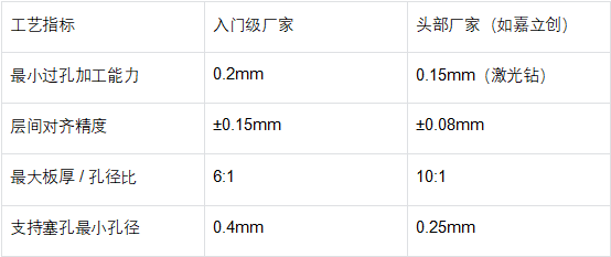
Manufacturer Process Capability Comparison and Selection Recommendations
The precision of different manufacturers’ equipment and their process experience directly affect the processing limits. For high multilayer PCB drilling, it is recommended to prioritize suppliers that meet the following conditions:
Conclusion: Drilling Design Self-Check List
Controlling the quality of drilling in high multilayer PCBs must run through the entire design process. It is recommended to check against the following points before mass production:
- Is the via diameter ≥ the minimum hole diameter promised by the manufacturer?
- Do the hole spacing and ring width meet the minimum safety distance?
- Is the length-to-width ratio of slot holes ≥2.5, and is the ring width up to standard?
- Are additional process requirements for special substrates indicated?
- Is a complete stack structure and hole position distribution diagram provided?
Following these specifications can not only reduce the defect rate of drilling to below 5% but also significantly shorten the prototyping cycle. It is recommended to save this article as a quick reference manual for high multilayer PCB drilling design, and it is essential to conduct a special review with the manufacturer’s process engineers before actual production.