Welcome to leave a message, I will reply to each message on the same day, and any errors in the article will be updated in the reply. The design is conducted in the Vivado 2018.3 environment, with specific code and detailed line-by-line comments at the end.
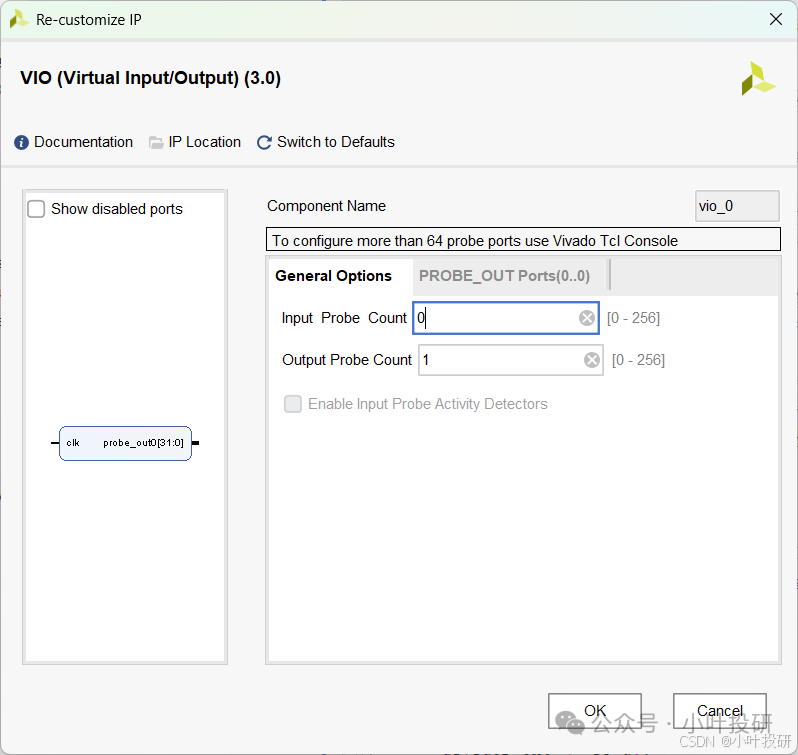
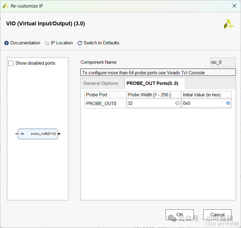
This is a dynamic display design for FPGA seven-segment displays, including the following modules: top-level design modulehex_top, as well as instantiated moduleshc595_driver and hex8, and also uses the IP corevio_0. The vio_0 has only one virtual output (signal width is 32, initial value is hexadecimal 0). Additionally, there is a simulation module for hex8 called hex8_tb.
The top-level module hex_top connects the VIO IP core (providing 32-bit display data disp_data), the display control module hex8 (which decomposes disp_data into 8 sets of 4-bit BCD codes, dynamically enabling 8 seven-segment displays through a 1kHz scanning clock and generating segment selection signals seg and digit selection signals sel) and the HC595 driver module hc595_driver (which concatenates {seg, sel} into 16-bit data, generates shift clock sh_cp and storage clock st_cp through a divided clock, and serially outputs data to the HC595 chip to complete latching); the simulation module hex8_tb verifies the digit selection and segment selection logic of hex8 by generating reset, clock, and multiple sets of display data (such as 0x12345678), ensuring the accuracy of dynamic scanning and decoding, ultimately achieving stable display of the 8-digit seven-segment display.
1. Top-level module hex_top
1.1 Function
Connects virtual input/output (VIO), seven-segment display control module (hex8), and HC595 driver module (hc595_driver), achieving overall coordination of data flow and hardware driving.
1.2 Core Logic
1.2.1 Signal Connections
1. Inputs:
-
clk: 50MHz system clock, providing a synchronous reference for all modules.
-
reset_n: Reset signal (active low), initializes each module.
2. Outputs:
-
sh_cp: HC595 shift clock, controls serial data shifting.
-
st_cp: HC595 storage clock, latches the shifted data.
-
ds: Serial data output, connected to the data input pin of HC595.
1.2.2 Module Instantiation
1. VIO IP core (vio_0):
-
Provides 32-bit virtual display data disp_data (initial value is 0x00000000), supports dynamic modification (e.g., input via software interface).
2. hex8 module:
-
Input: disp_data (data to be displayed), clk, reset_n, enable signal en (fixed at 1, always enables display).
-
Output: sel (8-bit digit selection signal), seg (7-segment selection signal).
3. hc595_driver module:
-
Input: clk, reset_n, data (concatenated {seg, sel}), enable signal s_en (fixed at 1).
-
Output: Timing signals driving HC595 (sh_cp, st_cp, ds).
1.2.3 Data Flow
-
vio_0.disp_data → hex8.disp_data → generates sel and seg → concatenates as {seg, sel} → hc595_driver.data → serially drives HC595 → seven-segment display.
1.3 Schematic of hex_top under RTL ANALYSIS

2. HC595 Driver Module hc595_driver: Hardware Timing Control
2.1 Function
-
Converts the segment selection (seg) and digit selection (sel) signals of the seven-segment display into serial data, driving the seven-segment display through the timing of the HC595 chip.
2.2 Core Logic
2.2.1 Input Processing
1. data:
16-bit input (high 8 bits for seg, low 8 bits for sel), cached through register r_data.
2. s_en:
Enable signal (fixed at 1), allows data input to be cached.
2.2.2 Clock Division
-
Division Counter: Divides the 50MHz clock by 2, generating approximately 25MHz shift clock (sck_plus), used to control the rhythm of serial data transmission.
2.2.3 Lookup Table Driving HC595
1. State Counting:
-
Counts the sck_plus pulses using SHCP_EDGE_CNT (0~32), corresponding to the 16-bit data transmission of HC595 (each bit of data requires 2 pulses: shift + latch).
2. Timing Logic:
-
Shift Phase (sh_cp): Sets sh_cp high on odd SHCP_EDGE_CNT, triggering the internal shift register of HC595 to receive ds data.
-
Latch Phase (st_cp): Sets st_cp high when SHCP_EDGE_CNT=32, latching the data from the shift register into the storage register, updating the display.
3. Data Output Order:
-
High bits first (r_data[15] to r_data[0]), complying with the serial input requirements of HC595.
3. Seven-Segment Display Control Module hex8: Dynamic Scanning and Decoding
3.1 Function
-
Converts 32-bit display data (8 sets of 4-bit BCD codes) into digit selection and segment selection signals, achieving dynamic scanning display.
3.2 Core Logic
3.2.1 Clock Division and Scanning Clock
-
Division Counter: Divides the 50MHz clock to generate a 1kHz scanning clock (period 1ms), used for dynamically switching the digit selection of the seven-segment display.
3.2.2 Digit Selection Signal Generation (Cyclic Shift Register)
1. 8-bit cyclic shift:
Under the drive of the 1kHz clock, sel_r starts from 0b0000_0001 (enabling the first seven-segment display), shifting left by one bit each time, sequentially enabling 8 seven-segment displays (returns to 0b0000_0001 after 0b1000_0000).
2. Enable Control:
As shown in the code below, ensures that all seven-segment displays are off when the enable is turned off.
sel = en ? sel_r : 8'b0000_00003.2.3 Data Selection and Segment Selection Decoding
1. Data Selection:
Selects the corresponding 4-bit BCD code from disp_data based on sel_r (e.g., sel_r=0b0000_0001 selects disp_data[3:0]), stored in data_tmp.
2. Segment Selection Decoding:
Converts the 4-bit BCD code into 7-segment display code using a case statement (e.g., 4’h0→7’b1000000 displays “0”).
3.3 Dynamic Scanning Principle
-
Each seven-segment display shows for 1ms/8=125μs, utilizing the persistence of vision effect, appearing as if 8 seven-segment displays are showing simultaneously.
-
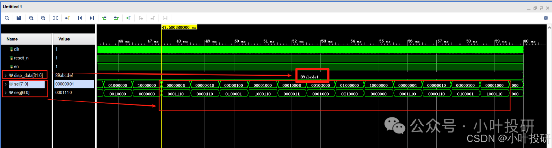
For example: when displaying 32’h12345678, the first seven-segment display shows 0x08 (disp_data[3:0]=8), the second shows 0x07 (disp_data[7:4]=7), and so on, achieving the overall display of “12345678” through rapid switching.
4. Simulation Module hex8_tb: Function Verification
4.1 Function
Generates stimulus signals to verify whether the digit selection and segment selection logic of the hex8 module is correct under different inputs.
4.2 Core Logic
4.2.1 Stimulus Generation
1. Clock:
20ns period (50MHz), consistent with the actual system.
2. Reset:
Initial reset is valid (reset_n=0), released after 20 clock cycles.
3. Display Data:
-
Initial value 32’h12345678 (displays “12345678”).
-
Switches to 32’h87654321 (displays “87654321”) and 32’h89abcdef (displays “89abcdef”).
4.2.2 Verification Points
-
Whether the digit selection signal sel cycles in order (0x01→0x02→…→0x80).
-
Whether the segment selection signal seg corresponds to data_tmp (e.g., when data_tmp=0x01, seg=0b1111001 displays “1”).
-
Whether the display switch correctly responds to changes in disp_data (e.g., switching from “12345678” to “87654321”).
4.3 Simulation Images
5. Summary
5.1 Data Input
VIO provides 32-bit display data, which is passed to hex8 by hex_top.
5.2 Dynamic Scanning
-
hex8 cycles through the seven-segment displays (sel) using a 1kHz clock, and extracts the corresponding 4-bit data (data_tmp) based on the current digit selection.
-
data_tmp is decoded to generate segment selection signal seg (e.g., displaying the number “1”).
5.3 Hardware Driving
-
hc595_driver concatenates seg and sel into 16-bit data, driving the seven-segment display through the serial interface of HC595.
-
sh_cp and st_cp control data shifting and latching, ensuring stable display.
5.4 Simulation Verification
-
hex8_tb simulates different inputs, verifying the digit selection and segment selection logic of hex8, ensuring consistency with expectations.
-
Key Advantages: Reduces hardware resource usage through dynamic scanning, utilizes HC595 for serial driving, supports flexible display of 8 seven-segment displays, suitable for scenarios requiring real-time updates of multiple characters (e.g., counters, status displays).
6. Code and Line-by-Line Comments for Operational Steps
6.1 Top-Level Module hex_top
// Description: Top-level file for hex8 project, coordinating the work and interfaces of VIO, hex8, and hc595module hex_top( input clk, //50MHz clock input reset_n, output sh_cp, //shift clock output st_cp, //storage clock output ds //serial data output); wire [31:0]disp_data; wire [7:0] sel; //digit selection (selects the current seven-segment display) wire [6:0] seg; //segment selection (current content to be displayed)vio_0 vio_0 ( .clk(clk), //50MHz clock .probe_out0(disp_data) );hc595_driver hc595_driver( .clk(clk), .reset_n(reset_n), .data({1'd0,seg,sel}), .s_en(1'b1), .sh_cp(sh_cp), //shift clock .st_cp(st_cp), //storage clock .ds(ds) //serial data output );hex8 hex8( .clk(clk), //50M, global clock .reset_n(reset_n), //reset signal, active low .en(1'b1), //seven-segment display enable, 1 for enable, 0 for off .disp_data(disp_data), //data to be displayed on 8 seven-segment displays, each 4 bits form a BCD code .sel(sel), //digit selection (selects the current seven-segment display) .seg(seg) //segment selection (current content to be displayed) );endmodule6.2 VIO Setup Interface
6.3 Driver Module hc595_driver
// Description: Drives hc595, outputs data and selection signalsmodule hc595_driver( input clk,// This driver follows ACX720 code style requirements, unifying code style, adjustments in case expressions, and should be noted when porting to other projects or chips input reset_n,// active low reset input [15:0]data,// data for 8 seven-segment displays' SEG and SEL input s_en,// seven-segment enable signal: 1 for enable, 0 for off output reg sh_cp,// shift clock output reg st_cp,// storage clock output reg ds // serial data output); wire reset=~reset_n;// changed to active high reset parameter CNT_MAX = 2;// set working clock, dividing the 50M clock by 2 reg [15:0]r_data;// input data register reg [7:0]divider_cnt;// division counter; wire sck_plus;// sck_plus is the divider count full flag reg [5:0]SHCP_EDGE_CNT;// counts sck_plus, used for lookup table to implement serial input of data and generate shift clock sh_cp and storage clock st_cp// Data register logicalways@(posedge clk)beginif(s_en)// When the enable signal is sent, cache the input data data r_data <= data;end// Division counter logicalways@(posedge clk or posedge reset)beginif(reset) divider_cnt <= 0;else if(divider_cnt == CNT_MAX - 1'b1) divider_cnt <= 0;else divider_cnt <= divider_cnt + 1'b1;end assign sck_plus = (divider_cnt == CNT_MAX - 1'b1);// sck_plus is the divider count full flag// sck_plus counting logicalways@(posedge clk or posedge reset)begin if(reset) SHCP_EDGE_CNT <= 0; else if(sck_plus)begin// Counts sck_plus, used for lookup table to implement serial input of data and generate shift clock sh_cp and storage clock st_cp. if(SHCP_EDGE_CNT == 6'd32) SHCP_EDGE_CNT <= 0; else SHCP_EDGE_CNT <= SHCP_EDGE_CNT + 1'b1; end else SHCP_EDGE_CNT <= SHCP_EDGE_CNT;end// Lookup table for state output logicalways@(posedge clk or posedge reset)beginif(reset)begin st_cp <= 1'b0; ds <= 1'b0; sh_cp <= 1'd0;end else begincase(SHCP_EDGE_CNT) 0: begin sh_cp <= 0; st_cp <= 1'd0;ds <= r_data[15];end // Store 1: begin sh_cp <= 1; st_cp <= 1'd0;end // Shift 2: begin sh_cp <= 0; ds <= r_data[14];end // Store 3: begin sh_cp <= 1; end // Shift 4: begin sh_cp <= 0; ds <= r_data[13];end // Store 5: begin sh_cp <= 1; end // Shift 6: begin sh_cp <= 0; ds <= r_data[12];end // Store 7: begin sh_cp <= 1; end // Shift 8: begin sh_cp <= 0; ds <= r_data[11];end // Store 9: begin sh_cp <= 1; end // Shift 10: begin sh_cp <= 0; ds <= r_data[10];end // Store 11: begin sh_cp <= 1; end // Shift 12: begin sh_cp <= 0; ds <= r_data[9];end // Store 13: begin sh_cp <= 1; end // Shift 14: begin sh_cp <= 0; ds <= r_data[8];end // Store 15: begin sh_cp <= 1; end // Shift 16: begin sh_cp <= 0; ds <= r_data[7];end // Store 17: begin sh_cp <= 1; end // Shift 18: begin sh_cp <= 0; ds <= r_data[6];end // Store 19: begin sh_cp <= 1; end // Shift 20: begin sh_cp <= 0; ds <= r_data[5];end // Store 21: begin sh_cp <= 1; end // Shift 22: begin sh_cp <= 0; ds <= r_data[4];end // Store 23: begin sh_cp <= 1; end // Shift 24: begin sh_cp <= 0; ds <= r_data[3];end // Store 25: begin sh_cp <= 1; end // Shift 26: begin sh_cp <= 0; ds <= r_data[2];end // Store 27: begin sh_cp <= 1; end // Shift 28: begin sh_cp <= 0; ds <= r_data[1];end // Store 29: begin sh_cp <= 1; end // Shift 30: begin sh_cp <= 0; ds <= r_data[0];end // Store 31: begin sh_cp <= 1; end // Shift 32: st_cp <= 1'd1; // Storage completedefault: begin st_cp <= 1'b0; ds <= 1'b0; sh_cp <= 1'd0; end endcaseendendendmodule6.4 Seven-Segment Display Control Module hex8
// Description: Generates division signals, segment selection and digit selection signals, outputs the data to be displayed, segment selection and digit selection valuesmodule hex8( input clk, //50M, global clock input reset_n, //reset signal, active low input en, //seven-segment display enable, 1 for enable, 0 for off input [31:0]disp_data,// data to be displayed on 8 seven-segment displays, each 4 bits form a BCD code output [7:0] sel,// digit selection (selects the current seven-segment display) output reg [6:0] seg// segment selection (current content to be displayed)); wire reset=~reset_n;// changed to active high reset reg [14:0]divider_cnt;// maximum value of counter=25000-1 reg clk_1K;// divider_cnt changes once when reaching 24999 (0.5ms), period is 1ms reg [7:0]sel_r; reg [3:0]data_tmp;// data cache, 4bit// Division counter counting module, preparing for obtaining 1KHz scanning clockalways@(posedge clk or posedge reset)beginif(reset) divider_cnt <= 15'd0;else if(!en)// not sending seven-segment display enable divider_cnt <= 15'd0;else if(divider_cnt == 24999) divider_cnt <= 15'd0;else// sending seven-segment display enable divider_cnt <= divider_cnt + 1'b1;end // 1KHz scanning clock generation module, preparing for 8-bit cyclic shift register always@(posedge clk or posedge reset)beginif(reset) clk_1K <= 1'b0;else if(divider_cnt == 24999)// flip clock when reaching 24999 clk_1K <= ~clk_1K;else clk_1K <= clk_1K;end// 8-bit cyclic shift register, preparing for sel and data_tmpalways@(posedge clk_1K or posedge reset)begin// Execute on the rising edge of the scanning clockif(reset)// On reset, switch to seven-segment display 0 sel_r <= 8'b0000_0001;else if(sel_r == 8'b1000_0000)// When reaching seven-segment display 7, return to seven-segment display 0 sel_r <= 8'b0000_0001;else// Cycle shift on each rising edge of the clock sel_r <= sel_r << 1;endassign sel = (en)?sel_r:8'b0000_0000;// Two-way multiplexer: when seven-segment display is enabled, sel=sel_r; when seven-segment display is not enabled, sel= 8'b0000_0000always@(*)begin// Always execute case statement, cache data into 4bit data_tmpcase(sel_r)// 8-to-1 multiplexer, delivering data to be displayed to the corresponding seven-segment display8'b0000_0001:data_tmp = disp_data[3:0];// data to be displayed on the first seven-segment display, four bits form a BCD code8'b0000_0010:data_tmp = disp_data[7:4];// data to be displayed on the second seven-segment display, four bits form a BCD code8'b0000_0100:data_tmp = disp_data[11:8];// data to be displayed on the third seven-segment display, four bits form a BCD code8'b0000_1000:data_tmp = disp_data[15:12];// data to be displayed on the fourth seven-segment display, four bits form a BCD code8'b0001_0000:data_tmp = disp_data[19:16];// data to be displayed on the fifth seven-segment display, four bits form a BCD code8'b0010_0000:data_tmp = disp_data[23:20];// data to be displayed on the sixth seven-segment display, four bits form a BCD code8'b0100_0000:data_tmp = disp_data[27:24];// data to be displayed on the seventh seven-segment display, four bits form a BCD code8'b1000_0000:data_tmp = disp_data[31:28];// data to be displayed on the eighth seven-segment display, four bits form a BCD codedefault:data_tmp = 4'b0000;// default data to be displayed is 4'b0000, i.e., not displayed.endcaseend// Encode and decode numbers or characters always@(*)begin// seg: segment selection (current content to be displayed)case(data_tmp)// Decode the corresponding output display based on the input 4bit data_tmp4'h0:seg = 7'b1000000;4'h1:seg = 7'b1111001;4'h2:seg = 7'b0100100;4'h3:seg = 7'b0110000;4'h4:seg = 7'b0011001;4'h5:seg = 7'b0010010;4'h6:seg = 7'b0000010;4'h7:seg = 7'b1111000;4'h8:seg = 7'b0000000;4'h9:seg = 7'b0010000;4'ha:seg = 7'b0001000;4'hb:seg = 7'b0000011;4'hc:seg = 7'b1000110;4'hd:seg = 7'b0100001;4'he:seg = 7'b0000110;4'hf:seg = 7'b0001110;endcaseendendmodule6.5 Simulation Module hex8_tb
/*Description: Tests the hex8 file, observing whether the output data, segment selection, and digit selection signals are generated normally, as well as the initialization and switching of reset signals and enable signals, displaying "12345678", "87654321", and "89abcdef" on the seven-segment display*/`timescale 1ns/1ns`define clk_period 20module hex8_tb; reg clk; //50M reg reset_n;// reset signal, active low reg en; // seven-segment display enable, 1 for enable, 0 for off reg [31:0]disp_data;// data to be displayed on 8 seven-segment displays, each 4 bits form a BCD code wire [7:0] sel;// digit selection (selects the current seven-segment display) wire [6:0] seg;// segment selection (current content to be displayed)hex8 hex8( .clk(clk), .reset_n(reset_n), .en(en),// seven-segment display enable, 1 for enable, 0 for off .disp_data(disp_data), .sel(sel), .seg(seg) );initial clk = 1;// initial clock set high always#(`clk_period/2) clk = ~clk;// toggle every 10ns, period is 20nsinitial begin reset_n = 1'b0;// trigger reset en = 1;// send seven-segment display enable disp_data = 32'h12345678;// right side is hexadecimal, each digit == 4 bits binary, total 32 bits binary #(`clk_period*20);// after 20 clock cycles reset_n = 1;// reset invalid #(`clk_period*20);// after another 20 clock cycles #20000000;// after 20000000ns disp_data = 32'h87654321;// right side is hexadecimal, each digit == 4 bits binary, total 32 bits binary #20000000;// after 20000000ns disp_data = 32'h89abcdef;// right side is hexadecimal, each digit == 4 bits binary, total 32 bits binary #20000000;// after 20000000ns $stop; endendmodule