With the continuous development of electronic information technology, semiconductor materials have undergone several iterations.Currently, the third-generation semiconductors represented by GaN and SiC have become a “battleground” for countries around the world, widely used in the manufacture of various electronic and optoelectronic devices.However, in recent years, new application scenarios such as 6G communication, super-fast charging for electric vehicles, ultra-high voltage transmission, and large-scale energy storage have emerged continuously. The physicochemical properties of third-generation semiconductors can no longer meet the higher performance requirements, thus the fourth-generation ultra-wide bandgap semiconductor materials represented by aluminum nitride (AlN), gallium oxide (Ga2O3), diamond, and boron nitride (BN) have begun to receive widespread attention. Fourth-generation semiconductors possess superior physicochemical properties, especially a bandgap that far exceeds that of third-generation semiconductors, demonstrating vast application potential in power electronics, RF electronics, and deep ultraviolet optoelectronic devices.
01
From First Generation to Fourth Generation Semiconductors
Since the invention of the transistor in 1947, every innovation in semiconductor materials has brought about a wave of large-scale industrial upgrades, from the first-generation semiconductors (Si, Ge), to the second-generation semiconductors (GaAs, InP), and to the third-generation wide bandgap semiconductors (GaN, SiC) that have gained much attention in recent years. In the past two decades, the design and manufacturing technologies of third-generation semiconductors have matured, and their applications in RF electronics, power electronics, and LEDs have been successfully commercialized on a large scale.
However, various electronic devices based on third-generation semiconductors are approaching their theoretical performance limits. To address the new challenges posed by more stringent electrical and optical application scenarios in the future, academia and industry are conducting cutting-edge technology research around ultra-wide bandgap semiconductors (UWBG). Representative ultra-wide bandgap semiconductors include aluminum nitride (AIN), gallium oxide (Ga2O3), diamond, and boron nitride (BN), which are referred to as “fourth-generation semiconductors” in the domestic industry. Fourth-generation semiconductors exhibit excellent physicochemical characteristics, including a bandgap far exceeding that of third-generation semiconductors, ultra-high breakdown electric fields, excellent thermal stability, and chemical inertness, showing outstanding advantages and application potential in ultra-high voltage power conversion, RF signal processing, deep ultraviolet optoelectronics, and extreme environment (radiation, high temperature) device technology.
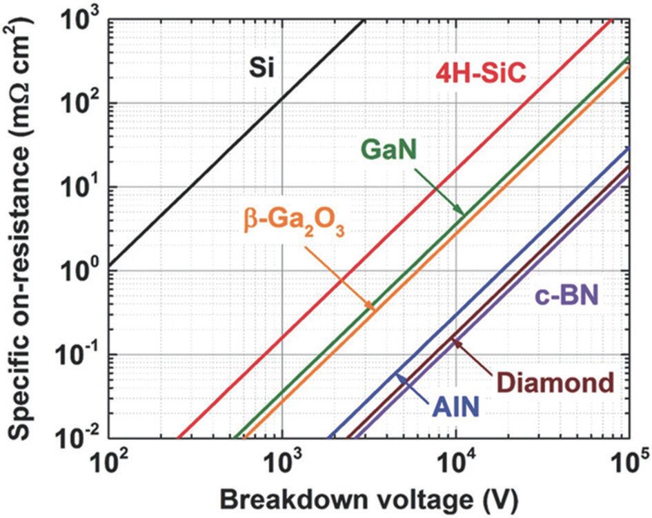
Figure 1 Performance improvements of typical semiconductor materials from the first to the fourth generation
(Image source: Advanced Electronic Materials)
02
Physical Properties of Typical Fourth Generation Semiconductor Materials
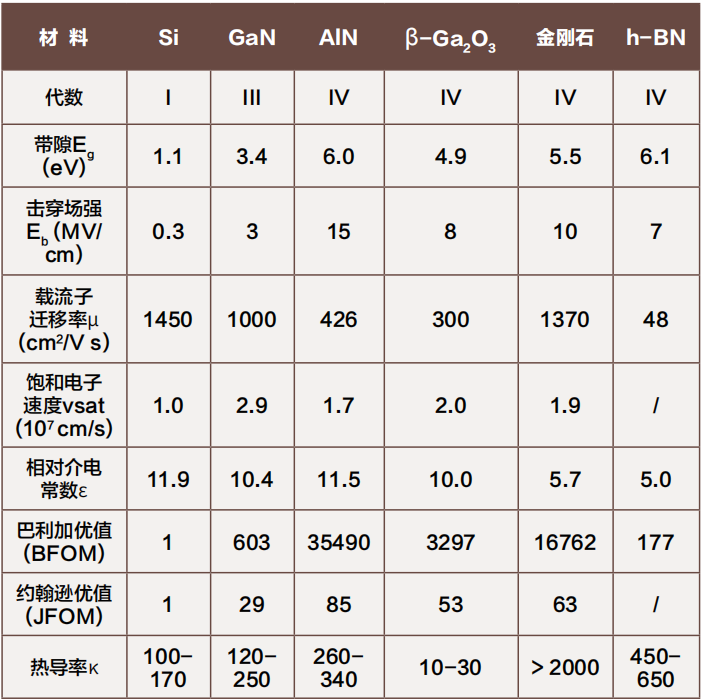
Table 1 horizontally compares the physical properties of typical fourth-generation semiconductors with traditional semiconductors (Si, GaN).Compared to first to third-generation semiconductors, the most intuitive advantage of fourth-generation semiconductors lies in their ultra-wide bandgap (Eg) and high breakdown field strength (Eb), allowing them to withstand the challenges posed by higher voltages and powers. Moreover, metrics such as Baliga’s figure of merit (BFOM) and Johnson’s figure of merit (TFOM), which measure the comprehensive performance of power electronics and RF electronic devices, tend to increase monotonically with Eg in a linear or even higher-order nonlinear manner, thus fourth-generation semiconductors exhibit overwhelming advantages. Specifically, BFOM is theoretically proportional to Eb3, and a larger value indicates that the corresponding low-frequency power device can carry more power with lower conduction loss, which means that fourth-generation semiconductors are particularly suitable for manufacturing high-power power electronic devices. At the same time, JFOM is roughly proportional to the breakdown field strength, and a larger parameter indicates a higher cutoff frequency and power output for RF amplifier devices, which also indicates that fourth-generation semiconductors are more suitable for manufacturing high-performance RF electronic devices.
However, aside from the aforementioned characteristics, fourth-generation semiconductors do not have significant advantages in other physical properties such as carrier mobility, saturation electron velocity, relative permittivity, and thermal conductivity. Considering the current mainstream application scenarios and production costs, fourth-generation semiconductors still cannot replace third-generation semiconductors in the short term.
Table 1 Comparison of the physical properties of typical semiconductor materials
(Image source: Progress in Quantum Electronics & Oxford Open Materials Science)
03
Applications and Current Issues of Fourth Generation Semiconductors
As mentioned earlier, the comprehensive performance indicators of fourth-generation semiconductors such as BFOM and TFOM exhibit overwhelming advantages compared to first to third-generation semiconductors. Therefore, in recent years, power electronics and RF electronic devices based on fourth-generation semiconductors have emerged like “mushrooms after rain.” Representative devices include AIN insulated gate bipolar transistors (IGBT), AIN metal-semiconductor field effect transistors (MESFET), β-Ga2O3 Schottky diodes (SBD), metal-oxide-semiconductor field effect transistors (MOSFET), β-(A11-xGax)O3/Ga2O3 high electron mobility transistors (HEMT), diamond SBDs, diamond MESFETs, and so on. These devices have gradually been applied in military radar, RF communication, electric vehicle charging piles, ultra-high voltage transmission, and other technical fields.
In addition, the absorption and emission spectral characteristic peaks of semiconductor materials are inversely proportional to Eg. Since the bandgap Eg of fourth-generation semiconductors is greater than 3.4 eV, optoelectronic devices made from these materials can operate in the deep ultraviolet range at wavelengths much shorter than 365 nm (the wavelength of GaN ultraviolet LEDs). These devices have many special applications, particularly in the UVC band (200-280 nm), where optoelectronic devices have considerable application potential in areas such as blind detection, ultraviolet lasers and LEDs, DUV lithography and micro-nano processing, medical diagnostics, and disinfection. Notably, during the growth of AIN, Ga ions can be introduced, and by adjusting the Al:Ga atomic ratio, AlGaN alloy materials can be produced. As the concentration of Ga changes, the bandgap of this material can be tuned between 3.4-6.0 eV, allowing its spectrum to cover most of the ultraviolet region, thus enabling tuning of the optoelectronic properties of devices according to actual application needs. This flexible tunable optoelectronic characteristic makes AlGaN the preferred material for blind detection devices.
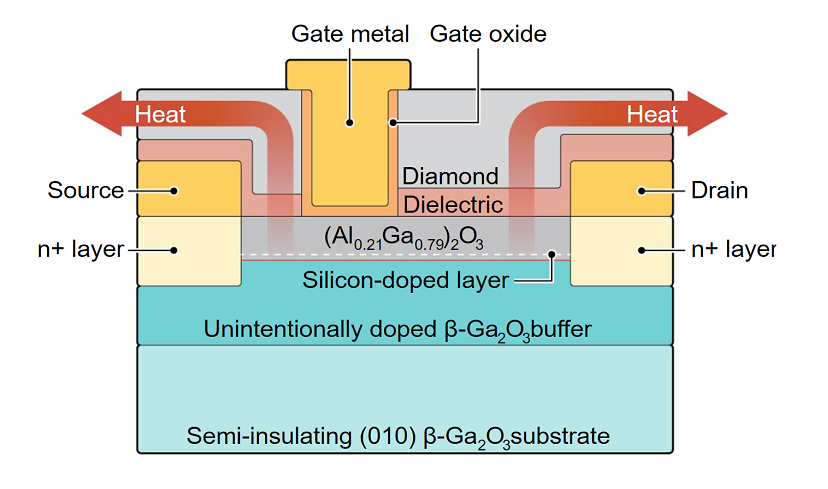
Figure 2 A typical β-Ga2O3 MOSFET power device
(Image source: Science)
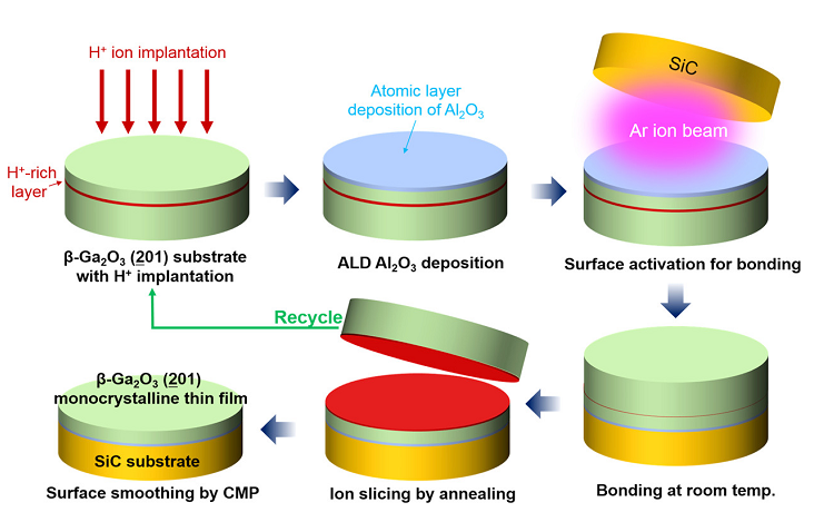
Figure 3 Heterogeneous integration of gallium oxide thin films and SiC high thermal conductivity substrates
(Image source: ACS Applied Materials & Interfaces)
In addition to the common applications mentioned above, these several fourth-generation semiconductors also have unique advantages, as the saying goes, “Eight Immortals cross the sea, each showing their own powers.”Among them, AIN is one of the materials with the most outstanding piezoelectric properties, making it very suitable for manufacturing RF front-end chips for 5G mobile phones, and it has been widely used in smartphones such as the iPhone. Diamond, being the material with the highest thermal conductivity in nature, has been used as a high thermal conductivity substrate for various high-power devices. Meanwhile, β-Ga2O3 has a simple production process, and its single crystal production cost is even lower than that of third-generation semiconductors like GaN, making it the most widely applied fourth-generation semiconductor currently.
Despite this, various fourth-generation semiconductors also have many limitations. Among them, the manufacturing process for AIN single crystal substrates is not yet mature, with dense lattice defects and small wafer sizes, leading to high manufacturing costs. Diamond, on the other hand, has excessive hardness, making it difficult to be compatible with existing semiconductor processing technologies, and the production cost of single crystal substrates is extremely high, far from achieving large-scale industrialization. As for β-Ga2O3, its thermal conductivity is too low, and it is prone to cleavage along specific crystal planes under stress, which severely limits its reliability and lifespan in high-power scenarios. To improve the thermal performance of gallium oxide devices and enhance their reliability, a feasible solution is to use heterogeneous integration technology to prepare heterojunctions of β-Ga2O3 thin films and high thermal conductivity substrates like SiC, significantly reducing the thermal resistance of gallium oxide devices. The mainstream heterogeneous integration technologies include two methods: heterogeneous epitaxial growth and low-temperature bonding.
04
“Bottleneck” Issues in the Fourth Generation Semiconductor Field
In the field of fourth-generation semiconductors, there is still a certain gap between China and the world’s top levels. Taking AIN as an example, for more than a decade, any size AIN single crystal substrates have been on the embargo list against China. Due to the high difficulty of the production process, currently, there are very few organizations abroad capable of producing high-quality AlN single crystal wafers of 2 inches or more, with representative companies being HexaTech and Crystal IS from the United States, which basically monopolize the high-end product line of AIN. However, in recent years, domestic enterprises and research institutions such as Aoqi Optoelectronics, China Electronics Technology Group Corporation 46th Research Institute, Songshan Lake Laboratory, and Peking University have successively overcome the production process challenges of this material and reached world advanced levels, although their maturity and stability need further improvement. At the same time, single crystal gallium oxide and diamond were also listed in the export control list by the U.S. Department of Commerce in August 2022, prohibiting exports to China. These signs indicate that a new round of technological competition marked by fourth-generation semiconductors has quietly begun.
Currently, China is increasingly emphasizing the layout of the fourth-generation semiconductor industry, with relevant plans being gradually launched. In the “14th Five-Year Plan” development plan, the preparation technologies of materials such as aluminum nitride, gallium oxide, diamond, and boron nitride have been included in the national key research and development programs, receiving more attention and support at the national level. Breaking through the “bottleneck” issues in this field is imperative.
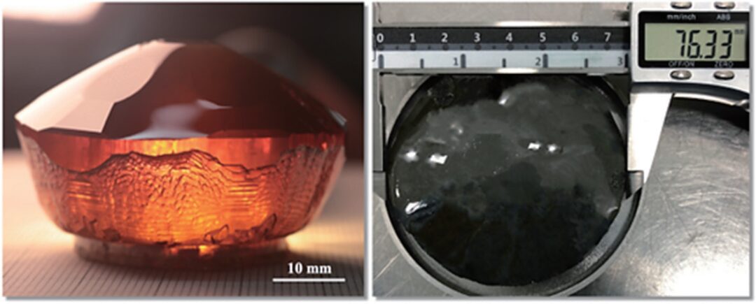
Figure 4 3-inch single crystal AIN ingots produced in China
(Image source: Aoqi Optoelectronics)
05
Summary and Outlook
“Materials, energy, and information” are the three pillars of human society, and semiconductors have undoubtedly become the common “cornerstone” of these three pillars. For this reason, every update and iteration of semiconductor materials drives an industrial upgrade and fundamentally transforms the development landscape of human society. Currently, semiconductors have developed to the fourth generation of ultra-wide bandgap semiconductors, with representative materials including aluminum nitride, gallium oxide, diamond, and boron nitride. These materials have extremely broad application prospects in information and energy technology fields, which has attracted the attention of countries worldwide and sparked a new round of technological competition globally. China has included fourth-generation semiconductor technology in the key research and development programs in the “14th Five-Year Plan,” and with strong support from the state, domestic enterprises and research institutions have made breakthrough progress in this field, generally reaching world advanced levels. It is believed that in the near future, China can completely overcome the “bottleneck” dilemma in the semiconductor field, breaking the monopoly of countries like Japan, the United States, and Europe, and becoming an important part of the global semiconductor industry landscape.
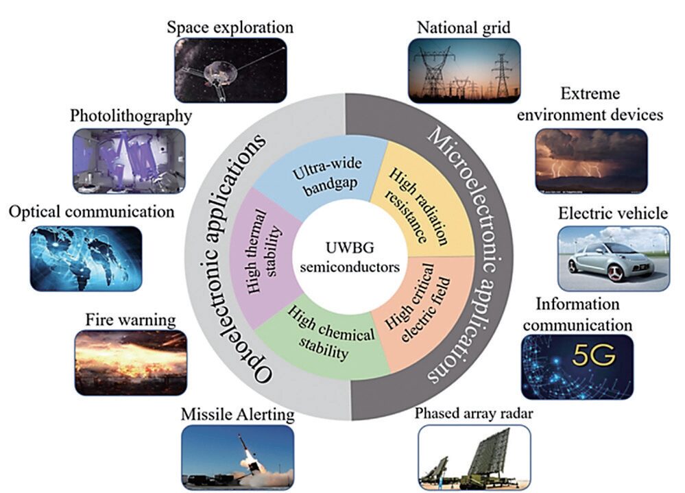
Figure 5 Typical application scenarios of fourth-generation semiconductors
(Image source: Progress in Quantum Electronics)
Author Information
Yang Guang, the author of this article, is a PhD student of the 2018 cohort at the School of Aerospace, Tsinghua University, with research interests in the phonon transport characteristics of semiconductors and their heterojunctions.
References:
[1] J.Y. Tsao, S. Chowdhury, M.A. Hollis, D. Jena, N.M. JohnsonK.A. Jones, R.J. Kaplar, S. Rajan, C.G. Van De Walle, E. Bellotti, C.LChua, R.Collazo, M.E.Coltrin, J.A.Cooper, K.R. Evans, S.Graham T.A.Grotjohn, E.R. Heller, M. Higashiwaki, M.S. Islam, PW. Juodawlkis, M.A. Khan, A.D. Koehler, J.H. Leach, U.K.Mishra, R.J. Nemanich, R.C.N. Pilawa – Podgurski, J.B.Shealy, Z. Sitar, M.J. Tadjer A.F. Witulski, M. Wraback, and J.A. Simmons. “Ultrawide – Bandgap Semiconductors: Research Opportunities and Challenges, ” Adv. Electron. Mater. 4(1),1600501 (2018).
[2] J. Yang, K. Liu, X. Chen, and D. Shen, “Recent advances in optoelectronic and microelectronic devices based on ultrawide-band-gap semiconductors, “Prog. Quantum Electron. 83, 100397 (2022).
[3] M. Xu, D.Wang, K. Fu, D.H. Mudivanselage, H. Fu, and Y. Zhao”A review of ultrawide bandgap materials: properties. synthesis and devices, “Oxf. Open Mater. Sci. 2(1), itac004 (2022).
[4] Q. Wang, D. Lei, J. Huang, X. Sun, D. Li, Z. Zhou, and L. Wu, “Homoepitaxial growth of 3-inch single crystalline AlN boules by the physical vapor transport process, “Front. Mater. 9, (2023).
[5] Z. Cheng, F. Mu, T. You, W. Xu, J. Shi, M.E. Liao, Y. Wang, KHuynh,T. Suga, M.S.Goorsky, X. Ou, and S. Graham, “Thermal transport across ion-cut monocrystalline β-Ga2O3 thin films and bonded β-Ga2O3-SiC interfaces,” ACS Appl Mater Interfaces, (2020).
[6] M.J. Tadjer, “Toward gallium oxide power electronics, “Science 378(6621),724 -725 (2022).
Reprinted content only represents the author’s views
Does not represent the position of the National Nano Center