
Bluetooth has always been a standard feature of smart devices, whether it is smartphones, laptops, or tablets. With the development of mobile internet, a large number of smart wearable devices have emerged. The development of these applications not only requires mobile software support but also relies on wireless sensing technology, with Bluetooth remaining the preferred communication method for wireless connections.
Bluetooth technology is the most crucial component in this context. It requires not only communication sensitivity but also miniaturization, low power consumption, and importantly, low cost.
The emergence of Bluetooth 4.0 version addresses these issues, which includes Bluetooth Smart (low energy) features with the following characteristics:
1) Low energy consumption
2) Low cost
3) Standard button batteries can power devices for years
4) Multi-vendor interoperability
5) Enhanced range
In hardware design, antenna design is quite critical. A commonly used low-cost design method is the PCB onboard antenna design. But how should PCB onboard antennas be designed in practice to achieve good transmission and reception effects? Below are four Bluetooth antennas design options for reference:
Bluetooth Antenna Design: Inverted F Antenna:
The inverted F antenna can be linear or planar. When using insulation materials with a high dielectric constant, the size of the Bluetooth antenna can be reduced. As a type of onboard antenna, the inverted F antenna design is low-cost but increases in size, making it the most common in practical applications. The antenna is generally placed on the top layer of the PCB, with the ground plane also on the top layer and located near the antenna; however, there must be no ground plane surrounding the antenna, and it should be a clear area. As shown in the figure below:
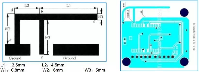
Figure 1: Inverted F Antenna Design Schematic
Bluetooth Antenna Design: Curved Antenna Design:
The length of the curved antenna is relatively difficult to determine. It is generally slightly longer than a quarter wavelength, and its length is determined by its geometric topology and ground plane. The curved antenna is generally PCB packaged, i.e., an onboard antenna. Similar to the inverted F antenna, the antenna is generally placed on the top layer of the PCB, with the ground plane also on the top layer and located near the antenna; however, there must be no ground plane surrounding the antenna, and it should be a clear area. As shown in Figures 2 and 3:
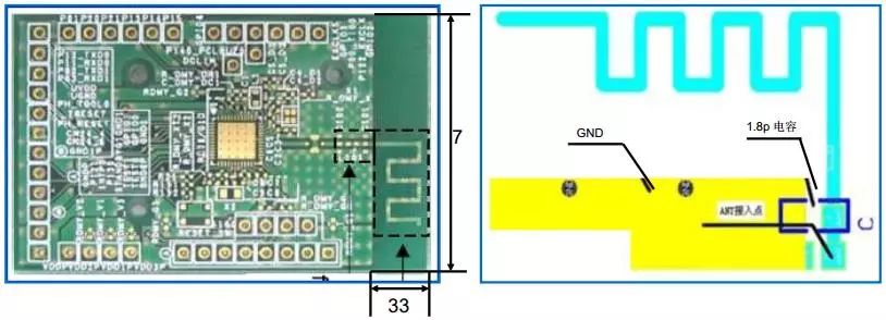
Figure 2: Curved Antenna Design Schematic 1
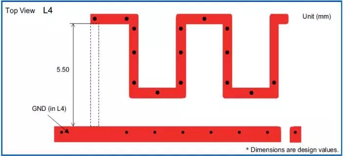
Figure 3: Curved Antenna Design Schematic 2
Note: Antenna length calculation formula:
Antenna length (meters) = (300/f) * 0.25 * 0.96
Where f represents frequency (MHz), and 0.96 is the wavelength shortening rate.
The length of the Bluetooth antenna is approximately 300/2.4G * 0.25 * 0.96, which is about 31mm.
Bluetooth Antenna Design: Ceramic Antenna Design:
Ceramic antennas are another type of miniaturized antenna suitable for Bluetooth devices. Ceramic antennas can be categorized into block ceramic antennas and multilayer ceramic antennas. Due to the higher dielectric constant of ceramics compared to PCB circuit boards, using ceramic antennas can effectively reduce antenna size. In terms of dielectric loss, ceramic media also have lower dielectric losses than PCB circuit boards, making them very suitable for low power Bluetooth modules. In PCB design, the area around the antenna should be clear, and it is particularly important not to place copper. As shown in the figure below:
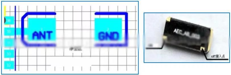
Figure 4: Ceramic Antenna Design Schematic
Bluetooth Antenna Design: 2.4G Stick Antenna Design:
The 2.4G stick Bluetooth antenna is large in size but has a transmission distance superior to other antennas. In PCB design, the area around the antenna must also be clear, similar to the three antenna designs mentioned above. As shown in the figure below:
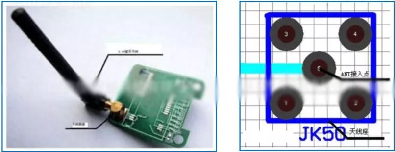
Figure 5: 2.4G Stick Antenna Design Schematic
Other Related Considerations for Bluetooth Antenna Design:
1) The signal of the antenna (frequency above 400MHz) is prone to attenuation, therefore, the distance between the antenna and nearby ground should be at least three times the line width.
2) For microstrip lines and strip lines, the characteristic impedance is related to the thickness of the board layers, line width, vias, and the dielectric constant of the board material.
3) Vias can produce parasitic inductance, which can cause significant attenuation of high-frequency signals, so it is best to avoid vias when routing RF lines.
Source:Luoye Xiaoxiao RFsister Maker RF Space