1. Abstract
A single-chip microcomputer (Single-Chip Microcomputer) is a microcontroller that integrates CPU, RAM, ROM, timing, counting, and various interfaces into one. It is small in size, low in cost, powerful in function, and widely used in smart products and industrial automation. The 51 microcontroller is one of the most typical and representative microcontrollers. This graduation design aims to learn and apply it to develop both software and hardware capabilities.

2. Description
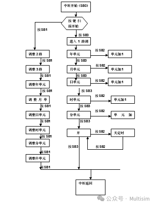
The system consists of the AT89C51, LED digital tubes, buttons, and light-emitting diodes, which can achieve functions such as time adjustment, setting timing, and output. The function selection of the system is completed by SB0, SB1, SB2, SB3, and SB4. Among them, SB0 is for time calibration and timer adjustment function key, pressing SB0 enters the adjustment state. SB1 is the function switch key. The first press of SB1 enters the prompt program for setting the timing for channel one, two, and three in sequence, and pressing SB3 enters the timing adjustment state for each channel. When the timing reaches, the diode lights up. After the cutoff time, it goes out. If you do not enter, continue pressing the SB1 key to sequentially enter the time calibration states for year, month, day, hour, minute, and second. Regardless of which state you enter, pressing SB2 can increment the adjusted position by 1 without carry. After all preset values are set, the system will store all settings in RAM, and pressing SB1 exits the adjustment state. After powering on, the system automatically enters the timing state, starting at 00:00:00. SB4 is the year, month, and day display conversion key, which can convert the original display of hours, minutes, and seconds to display year, month, and day.

3. Circuit Principle Analysis
1. Display Principle
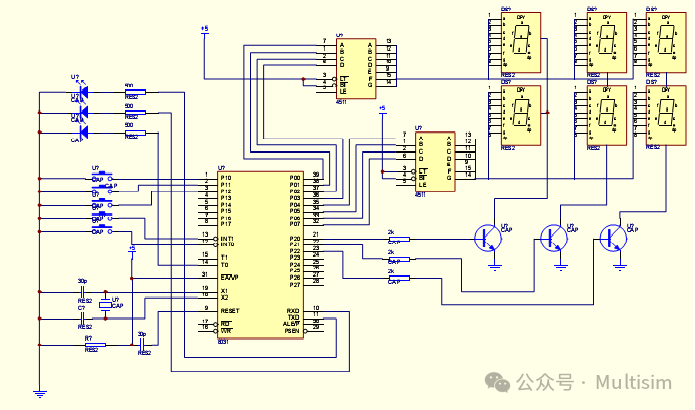
The circuit schematic is shown in Appendix 1. It consists of six common cathode digital tubes for displaying hours, minutes, and seconds. The eight data lines of port P0 from P0.0 to P0.7 are connected to the ABCD ports of two CD4511 decoders. The P2 port from P2.0 to P2.2 is connected to the bases of VT1 to VT3 through resistors R10 to R13. Thus, a high or low BCD display code of a storage unit is sent out through port P0, and the scanning selection code is sent out through port P2 to light up LED1 to LED6 in turn, displaying the data on the digital tube. The code output from port P0 is BCD code, and the output from port P2 is the position selection code. This is the principle of scanning display.
2. Keyboard and Reading Principle
The keyboard is the main device for human-computer interaction, and reading keys can easily cause misoperation. Software debouncing methods can be used to handle this. The software’s contact will produce bouncing when closing and opening, causing the logic level of the contact to be unstable. If not handled properly, it will lead to incorrect or repeated execution of key commands. Here, we use a software delay method to avoid bouncing, with a delay time of 20ms.
3. Implementation of Continuous Press Function
When a key is pressed, the corresponding function key explanation program is executed. If the operator does not release the key, the corresponding function will be executed repeatedly, as if executed continuously. Here, we use a software delay of 250ms. If the key is not released, the next corresponding program will be executed. Using the continuous press function allows for quick timing operations.

4. Program Design Philosophy and Related Instructions Introduction
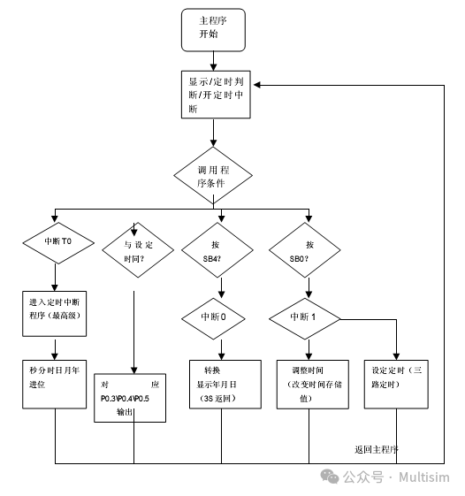
The main program of this system mainly completes the time display and timing output judgment functions. The display of year, month, and day, as well as the carry of each time unit, and the time setting functions are all completed in the interrupt service program.
1. Data and Code Conversion
As mentioned earlier, the position selection code is output from port P2, and the segment selection code is output from port P0, which will display numbers on the LED. However, the data output from port P0 is BCD code, while each storage unit stores binary numbers, which means that the data to be displayed does not correspond to the character representation. Therefore, directly sending the data of the storage unit to port P0 to drive the LED digital tube display is incorrect. The data to be displayed must be converted to BCD code internally in the system, and the segment selection codes of each unit’s data are sent to port P0, which is then decoded by CD4511 to drive the digital tube display.
The specific conversion process is as follows:
We first load the data to be displayed into the accumulator A, then convert the data in A into high and low BCD code, and then put it back into A, and finally output the value in A. For example, if a unit stores the number 45, it needs to be converted into four-digit BCD code: (0100)(0101), and then put into A. The high four bits in A represent 4, and the low four bits represent 5, which are sent to both decoders, and after decoding, the number 45 will be displayed on the two LEDs.
2. Implementation of Timing Function and Interrupt Service Program
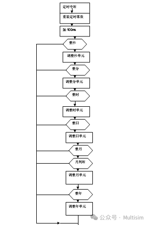
The operation of time relies on the timing interrupt subroutine to adjust the carry of the clock unit value. After the counter T0 is turned on, it enters the timing state, and after 100 milliseconds, it reloads the timer. After one interrupt, after one second, the second unit carries, and after 60 seconds, it becomes one minute, and the minute unit carries. After 60 minutes, the hour unit carries, and after 24 hours, the day unit carries. Thus, according to the carry rate, the values of year, month, day, hour, minute, and second storage units are obtained, and after decoding, they are sent to the LED for display, achieving the clock timing function. The increment is implemented using the INC instruction.
After entering the interrupt service program, execute PUSH PSW and PUSH A to save the contents of the program status register PSW and the data in the accumulator A. This is called “protecting the scene”. The storage area for storing critical data for protecting and restoring the scene is called the stack. Under software control, the stack can be set in any area of the internal RAM, and the data access of the stack is different from that of general RAM access. Operations on it must follow the “last in, first out” principle.
3. Time Control Function and Comparison Instructions
Another function of the system is to implement timing control of the execution device. The main control idea is as follows: first, set the opening and closing times of the execution device in a certain unit of RAM, and in the main timing program, execute several comparison instructions. If the current timing time is equal to the set opening time of the execution device, execute a CLR instruction to set the corresponding P3 to high level, turning it on; if the current timing time is equal to the set closing time of the execution device, execute SETB to set the corresponding P3 to low level, turning off the diode. The comparison instruction used to implement this control function is CJNE A, #direct, rel, which transfers if the value in the accumulator A is not equal to the immediate number.
References
1. Xie Zimei, “Electronic Circuit Design, Experiment, Testing” Wuhan: Huazhong University of Science and Technology Press, 2000
2. He Shusen, He Huabin, “Practical Digital Circuit Principles and Design” Fuzhou: Fujian Science and Technology Press, 2000.6
3. Bai Juyan, “Single-Chip Computer and Applications” Beijing: Electronics Industry Press, 1999.2

5. Program
SEC EQU 32H ;
MIN EQU 31H ;
HOUR EQU 30H ;
DAY EQU 35H ;
MON EQU 34H ;
YEAR EQU 33H ;
MIN_1 EQU 41H ;
HOUR_1 EQU 42H ;
DAY_1 EQU 43H ;
MON_1 EQU 44H ;
YEAR_1 EQU 45H ;
MIN_11 EQU 40H ;
HOUR_11 EQU 46H ;
DAY_11 EQU 47H ;
MON_11 EQU 48H ;
YEAR_11 EQU 49H ;
;***********************
ORG 0000H
ljmp MAIN
ORG 0003H ;
LJMP SHOW
ORG 000BH ;
LJMP TIME
ORG 0013H
LJMP CHANGE;
;——
MAIN:
;——–
MOV YEAR , #02
MOV MON , #05
MOV DAY , #01
MOV HOUR , #00
MOV MIN , #00
MOV SEC , #00
CLR 40H ;
CLR 41H
CLR 42H
CLR 43H
CLR 44H
CLR 45H
CLR 46H
CLR 47H
CLR 48H
CLR 49H
;——-
MOV TMOD , #01H ;
MOV TL0, #0B0H ;
MOV TH0, #3CH ;
clr p3.0
MOV 20H, #0AH ;
SETB PT0 ;
SETB TR0 ;
SETB ET0 ;
SETB EX0 ;
SETB EX1 ;
SETB EA ;
LOOP:
MOV R1, #30H;
MOV R4, #01H;
MOV R3, #03H;
NEXT:
MOV A , @R1 ;
MOV B , #10 ;
DIV AB
SWAP A
ORL A, B
MOV P0, A;
MOV P2, R4
INC R1 ;
MOV A, R4 ;
RL A ;
MOV R4, A
LCALL DE5SM ;
DJNZ R3, NEXT ;
CJNE R7, #88H,LOOP ;
MOV A, YEAR
CJNE A, YEAR_1, LOOP_1;
MOV A, MON
CJNE A, MON_1, LOOP_1
MOV A, DAY
CJNE A , DAY_1,LOOP_1
MOV A, HOUR
CJNE A, HOUR_1,LOOP_1
MOV A, MIN
CJNE A, MIN_1, LOOP_1
CPL P3.0
LOOP_1:
MOV A, YEAR
CJNE A, YEAR_11, LOOP;
MOV A, MON
CJNE A, MON_11, LOOP
MOV A, DAY
CJNE A , DAY_11,LOOP
MOV A, HOUR
CJNE A, HOUR_11,LOOP
MOV A, MIN
CJNE A, MIN_11, LOOP
CPL P3.0
LJMP LOOP
SHOW:
PUSH PSW
push ACC
PUSH B
PUSH 01H
PUSH 02H
PUSH 03H
PUSH 04H
MOV R2, #0FFH ;
TURN: MOV R1 , #33H
MOV R4 , #01H
MOV R3 , #03H
NEXT_1:
MOV A, @R1
MOV B , #10
DIV AB
SWAP A
ORL A, B
MOV P0, A
MOV P2, R4
INC R1
RL A
MOV R4 ,A
LCALL DE5SM
DJNZ R3, NEXT_1
DJNZ R2, TURN ;
POP 04H
POP 03H
POP 02H
POP 01H
POP B
POP ACC
POP PSW
RETI
TIME:
PUSH PSW
PUSH ACC
PUSH B
PUSH 06H
MOV TH0 , #3CH;
MOV TL0 , #0BH;
DJNZ 20H, OUT ;
MOV 20H, #0AH ;
INC SEC
MOV R6, SEC ;
CJNE R6, #60, OUT;
MOV SEC , #00 ;
INC MIN
MOV R6, MIN
CJNE R6, #60, OUT
MOV MIN , #00
INC HOUR
MOV R6 , HOUR
CJNE R6 , #25 , OUT
MOV HOUR ,#00
INC DAY
MOV R5, MON
CJNE R5, #1, MON_22;
MOV R5, DAY
CJNE R5, #32, OUT ;
INC MON
MOV DAY,#1
LJMP OUT
OUT:
POP 06H
POP B
POP ACC
POP PSW
RETI
MON_22:
MOV R5, MON
CJNE R5 , #2 , MON_33;
MOV A, YEAR ;
MOV B, #4
DIV AB
MOV A , B
JNZ OUT_1;
MOV R5 ,DAY
CJNE R5,#30, OUT;
INC MON
MOV DAY ,#1
LJMP OUT
OUT_1:
MOV R5, DAY
CJNE R5 ,#29, OUT ;
INC MON
MOV DAY , #1
LJMP OUT
END

6. Appendix
Experiment Design Circuit Diagram 1

Flowchart 1: Main Program Flowchart

Flowchart 2: Timing Interrupt Program Flowchart

Flowchart 3: Time Adjustment Function Flowchart


7. Experiment Insights
After two weeks of course design, I have gained many insights, particularly regarding microcontrollers and interpersonal relationships.
During this period, I received a lot of help from classmates. I was not very familiar with microcontrollers, and the things I learned seemed disconnected from reality. I struggled with the programming part due to my previous lack of understanding of assembly language. Later, I consulted a classmate, and every time we went to the lab together to debug the program, he explained things to me as he worked. Eventually, I successfully debugged it on the computer and later took some time to expand on it, completing this program.
Later, I found that I had developed a great interest in microcontrollers and wanted to buy some components to work on projects after returning home for the summer, as well as to improve my assembly language skills.
Finally, I would like to express my feelings about this course. The classroom teaching considers the needs of most students, emphasizing the “basics”—basic knowledge, basic theory, basic methods, and basic skills. This design provided us with an opportunity for in-depth learning and exploration, serving as a beneficial supplement to classroom teaching.

The End
Note:
Reply “Digital Clock” in the WeChat backend to obtain the original file.