The ELF 1 and ELF 1S development boards are compatible with the OV5640 camera, which integrates a CMOS image sensor. As a 5-megapixel camera, it supports image output with a maximum resolution of 2592×1944 (QSXGA) and a frame rate of up to 15fps. It also supports high-speed VGA (640×480) image capture at 90fps, demonstrating excellent capture speed and image processing performance.
By adjusting the internal register settings of the OV5640, users can easily enhance the image resolution, achieving image enlargement effects. However, it is important to note that as the ISP (Image Signal Processor) expands the range of processed images, the frame rate will correspondingly decrease to achieve the best balance between image quality and processing speed. This feature provides developers with flexible configuration options to adapt to diverse application scenarios.
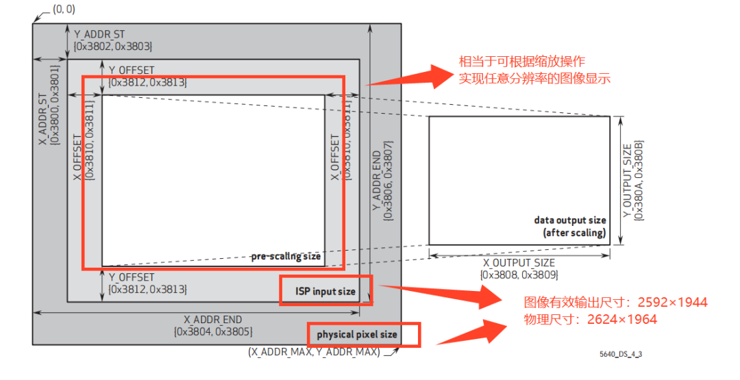
Introduction to the OV5640 Camera
The OV5640 camera integrates multiple functions, including Auto Exposure Control (AEC), Image Signal Processing (ISP), and Auto Focus Control (AFC), providing users with a comprehensive image optimization experience. Below is a functional block diagram of the OV5640 camera, visually presenting its core components and workflow:
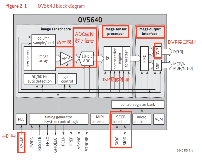
The ELF 1 development board has chosen the DVP interface as its image data transmission method. It is worth noting that while there are DVP modules on the market that support 10-bit data transmission, the ELF 1 development board only needs to receive the high 8 bits of data in practical applications, discarding the low 2 bits.
OV5640 Output Image Formats
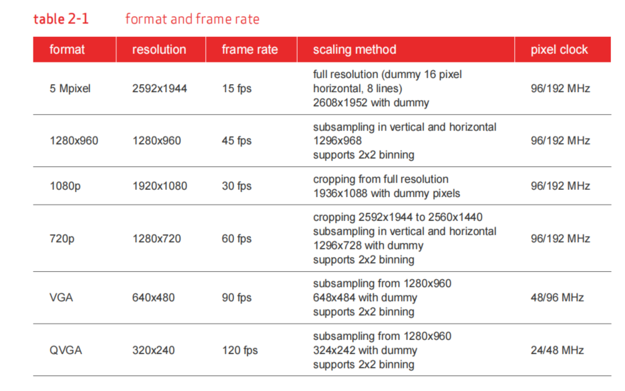
In addition to the image formats listed in the above image, the OV5640 camera also supports outputting images at any resolution below 2592×1944.
Hardware Circuit
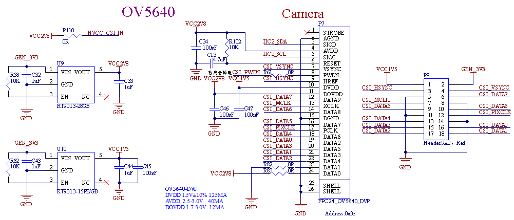
Below is the schematic diagram of the OV5640 module interface on the ELF 1 development board. The digital camera interface on the bottom board is connected to the OV5640 via an FPC connector, while the CSI signals are brought out through a 2.54mm pin header (P8).
OV5640 Power Control Timing Diagram
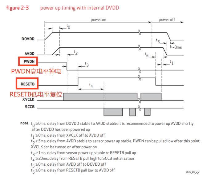
The above diagram shows the power-up timing diagram of the OV5640 camera, where the power-up sequence and precautions for each signal are as follows:
-
DOVDD and AVDD do not require self-designed power-up timing;
-
Since the high level of the OV5640_PWDN signal enables power-down, it can be set directly to 0 without delay;
-
The OV5640_RESETB low level resets and must be delayed for at least 1ms before it can be raised;
-
After raising the OV5640_RESETB, a delay of 20ms must be observed before proceeding with SCCB configuration;
