
Source: Tom Talks Chip Manufacturing
Original Author: Tom
Both 2D NAND and 3D NAND are types of non-volatile memory technology (NVM Non-Volatile Memory), which falls under the category of Memory. So, with 2D NAND available, why upgrade to 3D?
Definition
Non-volatile memory technology is a type of memory technology that retains stored data even when power is lost. Unlike volatile memory, non-volatile memory does not require a continuous power supply to maintain the stored data, including ROM (Read-Only Memory) and Flash Memory.Flash Memory, which is a type of non-volatile memory technology based on charge storage, is widely used in solid-state drives (SSD), USB flash drives, memory cards, and other devices. Flash Memory includes NOR and NAND types. NAND is further divided into 2D NAND and 3D NAND. 2D NAND, also known as planar NAND, has reached its capacity development limit. The growth of 2D NAND capacity is limited by how many memory cells can fit within a limited width and length. Since memory cells can only be arranged on a single plane, as storage capacity increases, the area of each memory cell decreases, leading to increased interference between memory cells, which can cause charge interference and data loss. The write speed of 2D NAND is relatively slow. During programming and erasing operations, it takes a longer time to inject or remove charge from the memory cells, resulting in delays in write operations.
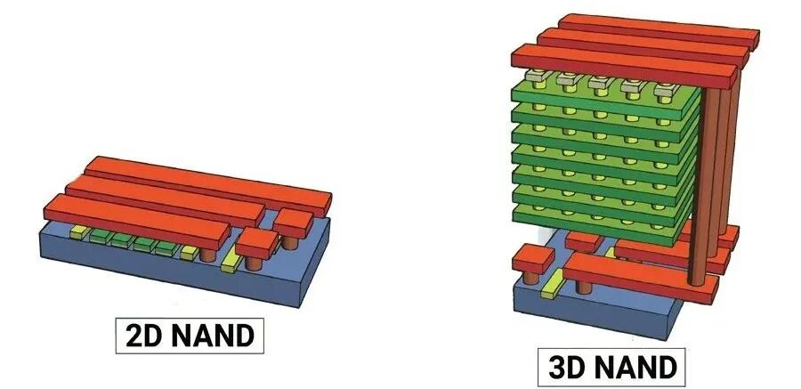
On the other hand, 3D NAND was developed to overcome the capacity limitations of 2D NAND. The 3D NAND architecture can scale to higher densities without sacrificing data integrity. Unlike 2D NAND, which stacks memory cells horizontally, 3D NAND uses multiple layers of vertical stacking to achieve higher density, lower power consumption, better durability, faster read and write speeds, and lower costs. By packaging so many vertical cells into smaller width and length dimensions, 3D NAND has a greater capacity than 2D NAND at the same length and width dimensions.
Comparison of Memory Cell Structures
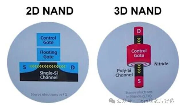 2.1 2D NAND Structure
- Control Gate: Located at the top, it controls the floating gate below. By controlling the voltage of the control gate, it can regulate whether electrons can enter or leave the floating gate.
- Floating Gate: Located below the control gate, wrapped in an insulating layer, it is used to store electrons. Electrons flow into or out of the floating gate to represent data as 1s and 0s.
- Single-Si Channel: This is the silicon channel connecting the source (S) and drain (D). Electrons flow through this channel from the source to the drain, controlled by the charge state of the floating gate, thus reading the stored information.
2.2 3D NAND Structure
- Control Gate: The control gate of 3D NAND is a three-dimensional structure that surrounds the storage pillars.
- Nitride: 3D NAND uses charge trap technology to store electrons. Electrons are stored in nitride, which is wrapped around the polysilicon channel, replacing the floating gate in 2D NAND. This charge trap layer gives NAND its non-volatile data storage capability.
- Poly-Si Channel: Unlike the single-crystal silicon channel in 2D NAND, the channel in 3D NAND is constructed vertically and made of polysilicon material, forming a three-dimensional storage pillar.
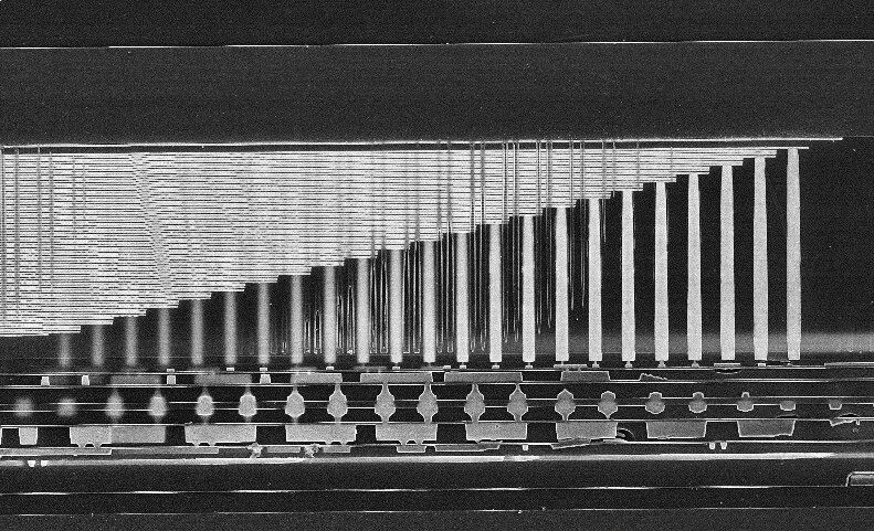
We further dissect the structure of 3D NAND, as shown in the figure: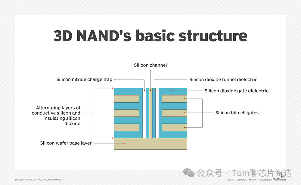
- Silicon Wafer Base Layer: This is the foundation of the 3D NAND structure, which is the silicon wafer.
- Silicon Bit Cell Gates: These are the gate structures that control the flow of electrons, determining whether electrons can enter or leave the silicon channel, thus enabling data storage and retrieval.
- Silicon Dioxide Gate Dielectric: This is the insulating layer located between the control gate and the silicon channel, which functions to maintain electrical isolation between the control gate and the silicon channel.
- Silicon Channel: The electrons flowing within are controlled by the voltage of the control gate, used for information storage.
- Silicon Dioxide Tunnel Dielectric: This allows electrons to flow into the silicon nitride charge trap during write operations via tunneling effect, and to be removed from the silicon nitride charge trap during erase operations.
ENDThe reproduced content only represents the author’s views and does not represent the position of the Semiconductor Institute of the Chinese Academy of Sciences.Editor: MarchEditor-in-Chief: Mu XinSubmission Email: [email protected]Previous Recommendations1. The Semiconductor Institute has made progress in the research of bionic covering neuron models and learning methods.2. The Semiconductor Institute has made significant progress in inverted structure perovskite solar cells.3. Why is copper used as interconnect metal in chips?4. What exactly is 7nm in chips?5. Silicon-based integrated optical quantum chip technology.6. How anomalous is the quantum anomalous Hall effect? It may lead to the next revolution in information technology!