Skip to content
Since my last article about the issue of counterfeit STM32 chips, ST has officially supported me by providing a batch of samples, including the STM32G473, for which I would like to express my gratitude to ST.
In this issue, we will design a development board using this chip.
The STM32G4 series is designed for applications requiring high performance, low power consumption, real-time control, and digital signal processing.The frequency can reach up to 170 MHz, and it features DSP and FPU instruction sets for efficient digital signal processing and mathematical calculations.

It greatly surpasses other chips in terms of analog peripherals.

From CubeMX, we can see that it has rich ADC and DAC resources, as well as multiple comparators and operational amplifiers, making this chip very rich in analog peripheral resources.

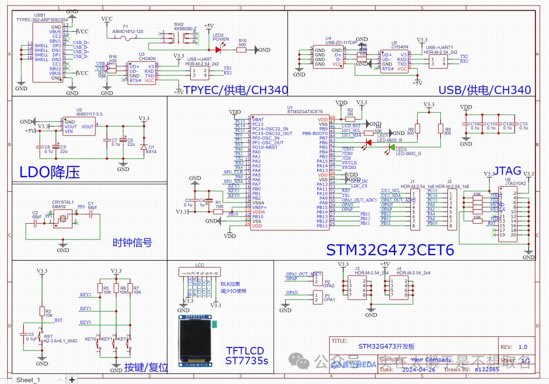
We use Lichuang EDA for schematic and PCB design, and here we will introduce the purpose and design of each part step by step.

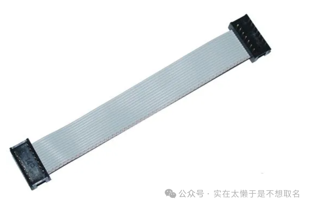
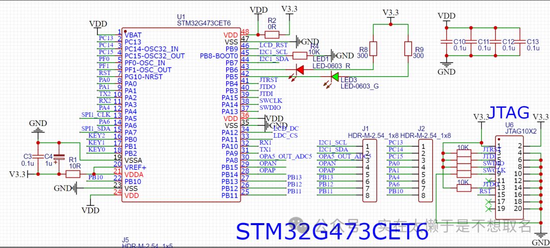
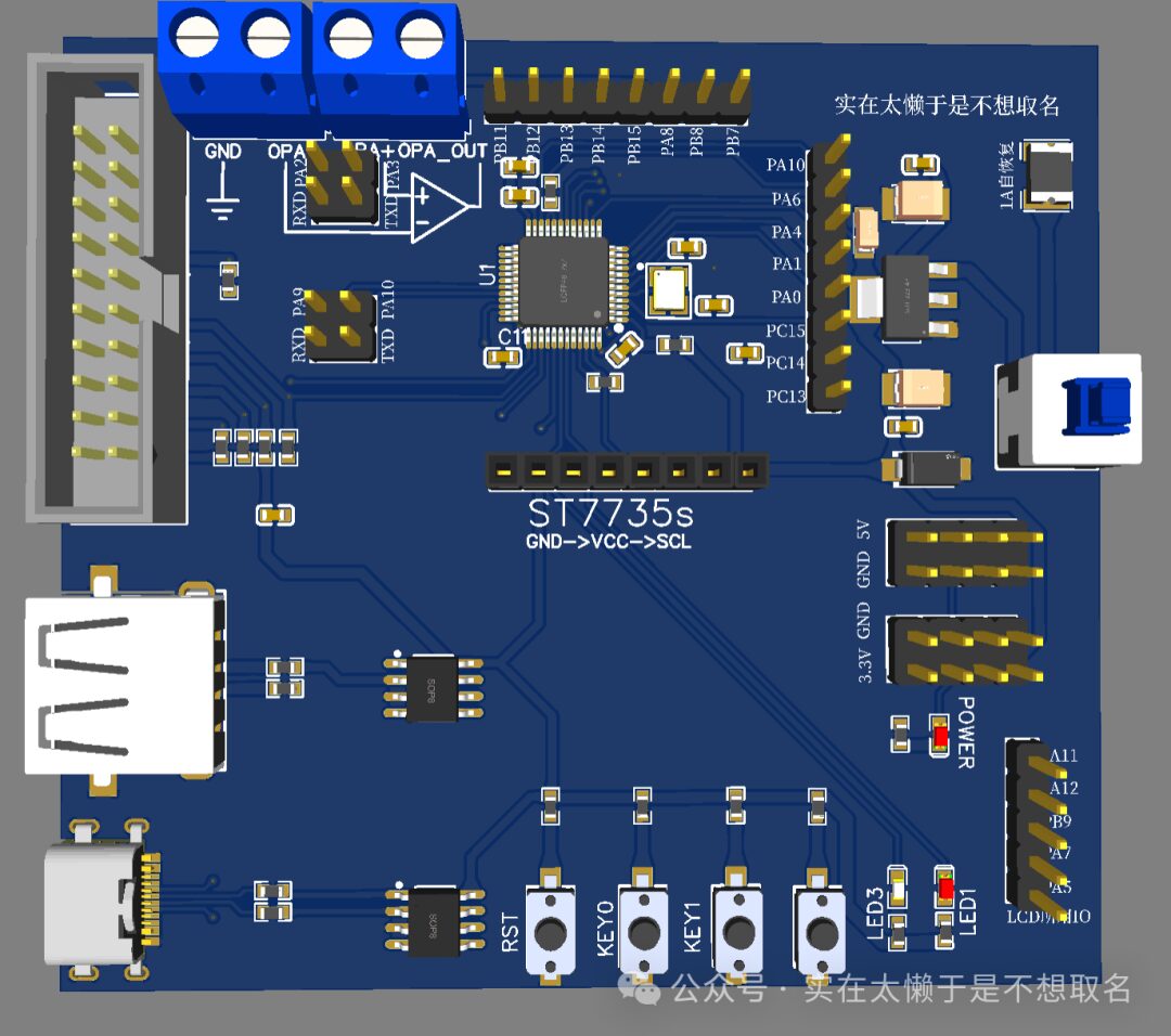
First is the downloading method, which usually uses a two-wire system combined with VCC and GND, making a total of four wires. However, I prefer to use a 20Pin ribbon cable for connection instead of Dupont wires.

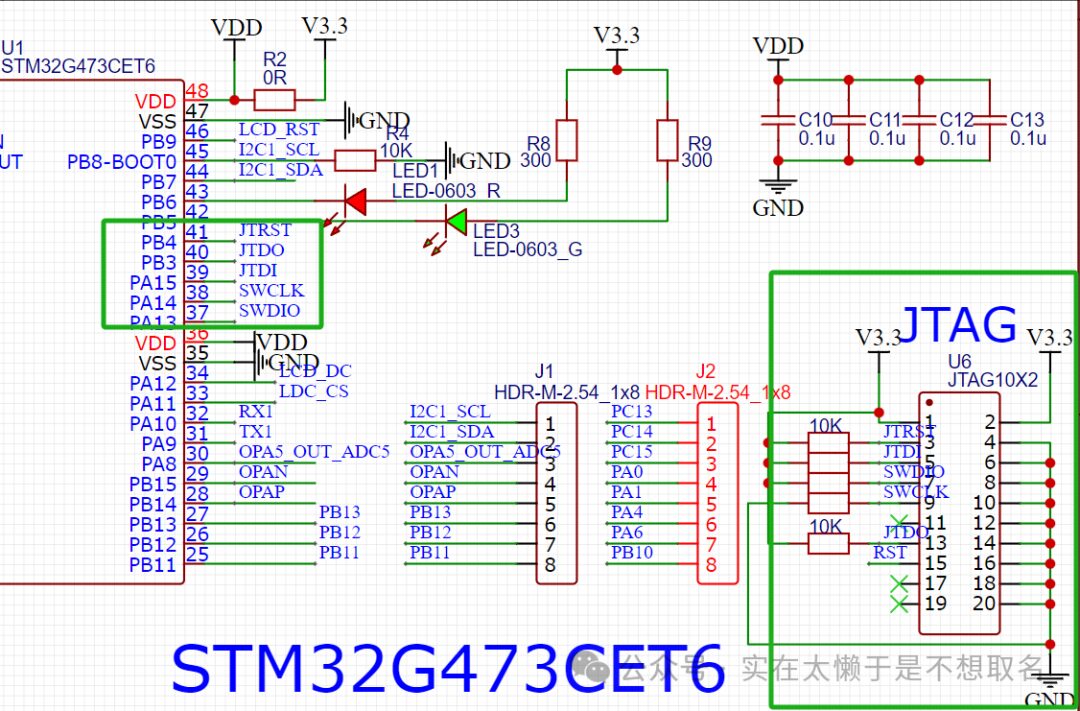
Therefore, I chose a 20Pin JTAG interface for connection, and the downloading method is also selected to be a five-wire system. Upon careful examination, I found that the additional IOs in five-wire downloading do not have very special functions since I mainly use its analog functions, and the extra three IOs do not have analog capabilities, so I simply opted for five-wire downloading.
-
Power Supply and Communication

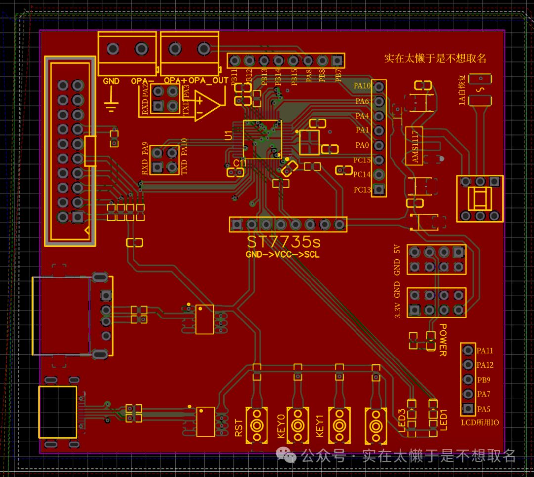
The power supply part selects a 16Pin Type-C power supply, with a 1A tripping self-resetting fuse to prevent excessive current, and a self-locking switch as the main switch.
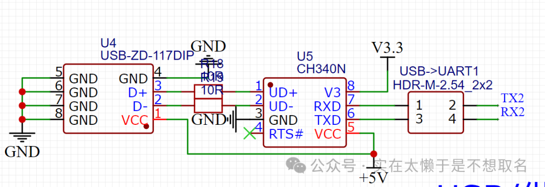
Communication with the microcontroller is done through the CH340 chip, which can be connected to Serial Port 1 via pin headers.

Similarly, there is also a USB device connected to Serial Port 2 of the STM32 via CH340, but this is a USB-A port, facilitating communication with other development boards.

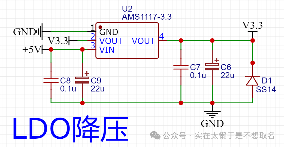
Finally, the AMS1117-3.3 LDO chip is used to convert 5V to 3.3V, with filtering capacitors and Schottky diodes added to suppress high-frequency signals.

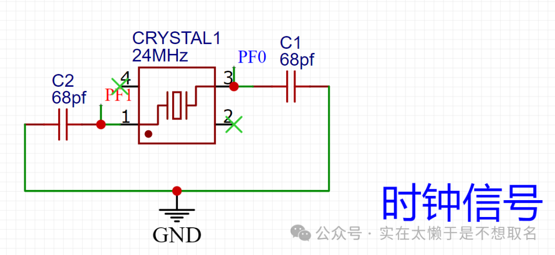
For the high-speed clock, a 24MHZ chip is selected, connected to PF0/PF1, and two small capacitors are used for filtering.
We will not add an additional low-speed clock source because it would occupy two IOs, and the IO resources on this board are quite limited.

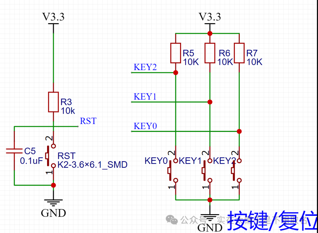
The reset IO is pulled up by a resistor. Originally, the three button IOs could be used without pull-ups by utilizing internal pull-ups or pull-downs, allowing us to reuse these three IOs as regular IOs.
As for the filter capacitors for the buttons, we chose not to add them, as we can choose to debounce in software, making the addition seem redundant.

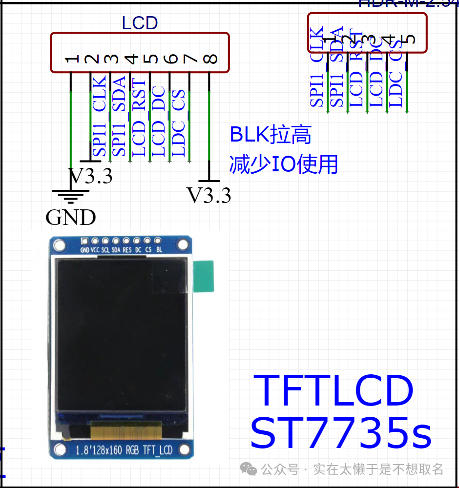
For the screen part, we chose TFTLCD, but we do not use parallel LCDs, as they occupy too many onboard IOs. If used, it would involve dozens of IOs. Instead, we use SPI communication, which combines control IOs to a maximum of 5 IOs, facilitating easy connection with pin headers (pin headers can also be used) and similarly leads out a set of pin headers.
-
External Power Supply and OPA

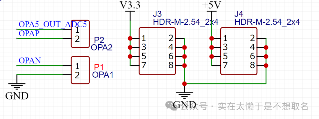
We designed two sets of 5V and 3.3V external power supplies to facilitate our board supplying power to modules. There are also two sets of interfaces because I specifically enabled an onboard OPAMP, which is an operational amplifier, and designed a set of interfaces for easy amplification circuit design or other circuits.

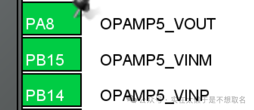
The PA8 can also be directly reused to ADC5, facilitating direct ADC sampling. Similarly, the operational amplifier can also be used as a controllable gain amplifier or a follower.

Finally, regarding the main control, it is important to adjust the resources of each IO properly, leading out the spare IOs (some already occupied can also be led out) to prevent decoupling capacitors from the chip, and setting two onboard LEDs for debugging convenience.


Here, my PCB drawing skills are not very deep, please bear with me.


