Professor Su Zhiqiang’s research group at Beijing University of Chemical Technology recently published a review article in the Chemical Engineering Journal, titled “Design strategies and applications of wearable piezoresistive strain sensors with dimensionality-based conductive network structures.“
Abstract: The design of conductive network structures in polymer conductive composites (PCC) and the selection of conductive nanofillers of different dimensions. This paper mainly discusses the impact of nanomaterial size on the performance of PCCs. Notably, nanomaterials of different dimensions can synergistically interact with PCCs to construct high-quality sensors. Subsequently, we summarize the effects of different structural designs, namely one-dimensional fibers, two-dimensional layered structures, and three-dimensional network structures, on the sensitivity, detection range, and cyclic stability of strain sensors. The applications of wearable piezoresistive strain sensors in physiological signal monitoring, disease treatment, healthcare, and human-computer interaction are discussed. Additionally, the challenges faced in using wearable piezoresistive strain sensors are explored.
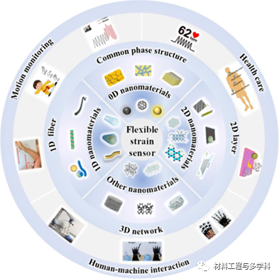
The selection of nanomaterials, the construction of conductive network structures, and the applications of wearable strain sensors.
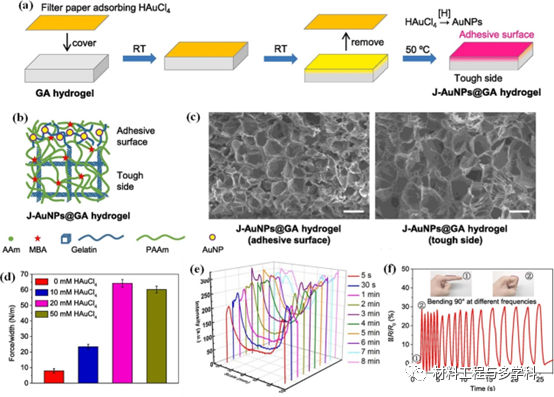
Figure 1(a) Schematic diagram of the preparation of J-AuNPs@GA hydrogel. (b) Schematic diagram of the structure of J-AuNPs@GA hydrogel. (c) SEM images of J-AuNPs@GA hydrogel on both sides. (d) Maximum adhesion strength of J-AuNPs@GA hydrogel on glass. (e) Distribution curve of AuNPs soaked in 4mM HAuCl4 for different times and then incubated at 50 °C for 12 hours in the hydrogel. (f) Resistance change of J-AuNPs@GA hydrogel during finger bending at different frequencies of 90 °.
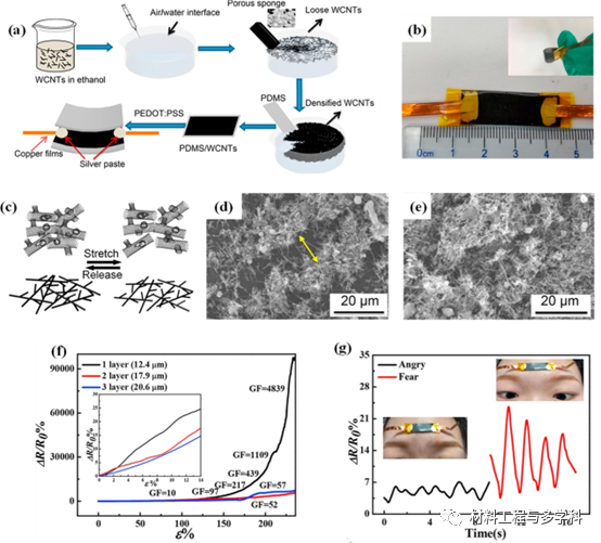
Figure 2(a) Preparation of WCNT nanocomposite films and schematic diagram of the structure of the strain sensor. (b) Image of the flexible strain sensor based on WCNT. (c) Schematic diagram of the three-dimensional network deformation of WCNT films during stretching and release. (d) Scanning electron microscope images of WCNT films during stretching and release. (e) Relative resistance change of WCNT sensors of different thicknesses during stretching. (f) Relative resistance change of carbon nanotube whisker sensors connected to the face.
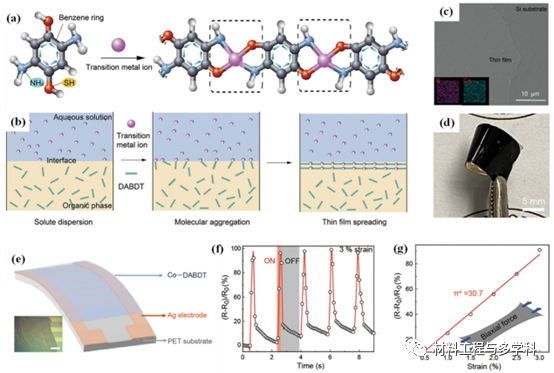
Figure 3(a) Chemical structure of metal-DABDT compounds. (b) Film formation process of metal-DABDT. (c) Scanning electron microscope image of Co-DABDT film. (d) Photo of a flexible device based on Co-DABDT film. (e) Schematic diagram of the Co-DABDT sensor device based on interdigitated electrodes. (f) Strain and resistance changes of Co-DABDT sensors over time. (g) Linear relationship between strain and resistance values.
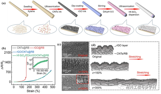
Figure 4(a) Schematic diagram of the preparation method of superhydrophobic conductive RB. (b) Change of relative resistance of the sensor with strain. (c) Surface scanning electron microscope image of PDA/rGO/CNTs@RB during stretching. (d) Schematic diagram of the slip of the conductive layer during stretching.
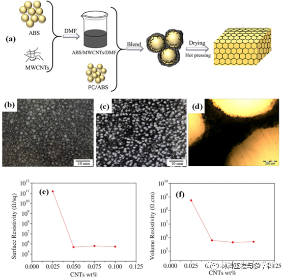
Figure 5(a) Schematic diagram of the composite material manufacturing process. (b) Optical photo of PC/ABS/MWCNTs samples prepared by solution-mechanical mixing method. (c) Plastic deformation generated during hot pressing, wrapped with polystyrene/multi-walled carbon nanotube polypropylene/polystyrene particles. (d) High-resolution image of PC/ABS/MWCNTs. Surface (e) and volume (f) resistivity of ABS/MWCNTs coated PC/ABS prepared by solution-mechanical mixing method.
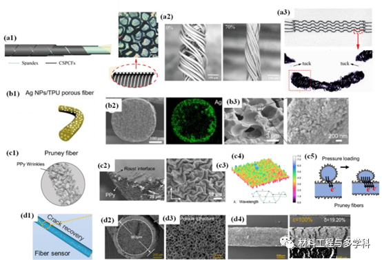
Figure 6(a1) Schematic diagram of the assembly structure of DCCY and cross-sectional micrograph of CSPCFs. (a2) In situ scanning electron microscope images of DCCY at 0% and 70% tensile strain range. (a3) Photo of the fabric sensor and micrograph of the arch-shaped DCCY inside the fabric sensor. (b1) Schematic diagram of Ag NPs/TPU porous fibers. (b2) Scanning electron microscope cross-section of Ag NPs/TPU porous fibers and EDS elemental mapping in Ag NPs/TPU porous fibers. (b3) SEM images of Ag NPs/TPU porous fibers at different magnifications. (c1) Schematic diagram of wrinkled fibers. (c2) SEM image of the cross-section of PPy@TPU wrinkled fibers. (c3) Surface SEM image of PPy@TPU wrinkled fibers prepared with 20mmol/L APS concentration. (c4) Schematic diagram of the three-dimensional morphology of PPy@TPU wrinkled fibers based on 5mmol/L APS concentration, illustrating its sensing mechanism. (d1) Schematic diagram of micro-crack structure of optical fiber sensor. (d2) Cross-section of core-sheath fiber. (d3) Porous structure of TPU in the inner layer of the fiber. (d4) Initial fiber and fiber with 100% stretch ratio.
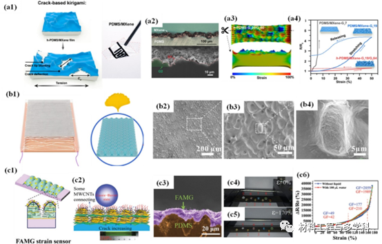
Figure 7(a1) Schematic diagram of crack-based kirigami film and crack evolution of h-PDMS/MXene film during stretching, along with a photo of PDMS/MXene film. (a2) Cross-sectional optical (top) and scanning electron microscope (bottom) images of PDMS/MXene film. (a3) Finite element method analysis of strain distribution in h-PDMS-G120/G260 film. (a4) Change in resistance of PDMS/MXene layered films with different ridge heights at a tensile strain of 50%. (b1) Schematic diagram of biomimetic piezoresistive sensor based on MXene. (b2), (b3), and (b4) are SEM images of biomimetic structural sensing elements based on MXene. (c1), (c2) Schematic diagrams showing how liquid interference is prevented in strain sensing and liquid wetting mode in FAMG strain sensors at 110%. (c3) High magnification SEM image of the cross-section of FAMG strain sensor. (c4) Optical photo of eight 100μL droplets on FAMG sensor stretched to (c4) ε = 0% and (c5) ε = 170%. (c6) Change in resistance with tensile strain, linear fitting on the surface of 100μL water and anhydrous FAMG sensor.
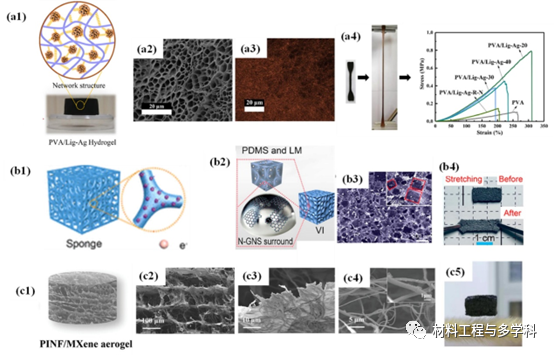
Figure 8(a1) Structural description of PVA/Lig-Ag hydrogel. (a2) SEM image of PVA/Lig-Ag-RN hydrogel. (a3) Elemental localization of silver in PVA/Lig-Ag hydrogel. (a4) Stress-strain curves of PVA/Lig-Ag hydrogel before and after stretching. (b1) Schematic diagram of sponge structure and scaffold unit. (b2) Schematic diagram of PDMS/LM/N-GNS sponge pressure sensor. (b3) Scanning electron microscope image from a top view. (b4) Photo of soft PDMS/LM/GNS sponge during stretching. (c1) Schematic diagram of PINF/MXene composite aerogel. (c2)-(c4) PINF/MXene composite aerogel at different magnifications, with the insert in (c4) showing high magnification SEM image of PINF wrapped with MXene. (c5) Digital image of PINF/MXene.
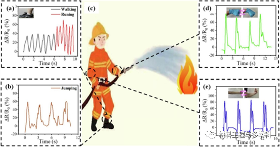
Figure 9(a) Resistance change curve of MFNC-8 fabric during walking and running, (b) jumping, (d) bending wrist and (e) bending elbow. (c) Application of Fabric-mfNC-8 on motion-sensing firefighting suits.
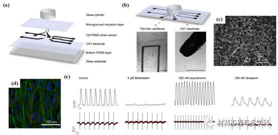
Figure 10(a) Schematic diagram showing the structure and components of a carbon-based biosensing platform. (b) Example image of cantilever deflection caused by myocardial cell contraction and example image of CNT electrodes covered by microgroove insulation layer. (c) SEM images showing the porous structure and surface morphology of CB-PDMS composites prepared by spray deposition method. (d) Confocal images of aligned iPSC-CM stained with α-actin. (e) Representative electrical readings of myocardial cell contraction amplitude and field potential curves before and after administering effective drug doses.
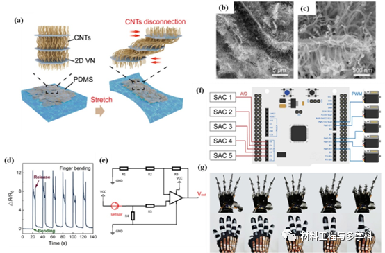
Figure 11(a) Schematic diagram of the breaking and reverse breaking of layered VN/CNT materials during stretching and release. (b) and (c) are typical SEM images of VN/CNTs composites with bristle structures. (d) Relative resistance change of the sensor when bending fingers. (e) The signal acquisition circuit includes an operational amplifier, a sensor, and five resistors. (f) The control circuit of the robotic hand control system includes five signal acquisition circuits (SAC), a microcontroller, and five servo circuits. (g) Photo of an instant-grasping robotic hand demonstrating gestures from “5” to “1”.
Thanks to the National Natural Science Foundation (51873016) for funding. XYZ thanks the Central University Basic Research Fund (ZY2103) for financial support.
https://doi.org/10.1016/j.cej.2022.140467