With the development of technology and the shift in military strategic thinking, unmanned aerial vehicles (UAVs) have a wide range of application prospects and extremely important practical significance in both military and civilian fields. Countries are developing various UAVs with unique performance, and the core of these modifications is the flight control system.
The DSP, with its rich instruction set, high-speed and high-precision computing capabilities, and abundant on-chip and off-chip resources, provides an excellent platform for the development of flight control systems. The TMS320F2812 (hereinafter referred to as F2812), selected for this system, is a 32-bit DSP chip developed by TI, utilizing high-performance static CMOS technology, with a maximum operating frequency of 150 MIPS. It integrates 128K words of FLASH memory, facilitating software upgrades; it also includes a variety of peripheral devices, such as a 12-bit 16-channel A/D converter with a sampling frequency of up to 12.5 MIPS, two event managers for motor control, and various standard serial communication peripherals. Based on this, a new flight control system with high precision, strong scalability, miniaturization, and low cost has been designed.

1. Hardware System Requirements and Design
The key to the hardware design of the DSP-based flight control system lies in the overall system design. Interface design is an important aspect that directly affects system performance. To reduce the system burden, external input signals are read in using interrupts, and the input and output of signals must consider anti-interference. Taking full advantage of the on-chip resources of the TMS320F2812 and the system’s interface requirements, only a small amount of external interface expansion is needed to meet all the functions and future scalability requirements of the flight control system. Additionally, due to the large number of input logic signals, an Altera CPLD chip EPM7128 is used to complete data processing and logical operations, reducing the size of the control circuit, increasing system reliability, and enabling monitoring and control of the status of each unit in the control system. The overall system design is shown in Figure 1. The following will explain the implementation of each module in the system.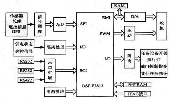

2. Hardware Implementation
2.1 Analog Signal Reception The analog signal is input through the signal conditioning module, and the A/D conversion selects a 12-bit successive approximation A/D converter AD1, which contains a tri-state output buffer circuit and a high-precision reference voltage source with a clock circuit, along with a built-in sample-and-hold circuit. The connection method used in this design is shown in Figure 2, allowing AD1 to operate in full control mode. The use of AD1 employs a program start and flag query method, where the start signal and conversion end signal are coordinated, ensuring that once AD1 completes the conversion, it enters the data output state and simultaneously generates an AD end flag, improving the throughput rate during multi-channel operation.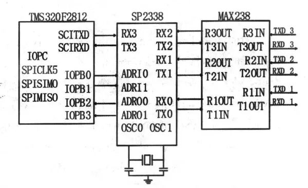 2.2 Serial Communication The F2812 processor provides two serial communication interfaces (SCI), supporting 16-level receive and transmit FIFO, but still does not meet the communication requirements of the flight control system with multiple peripherals. Therefore, the system selects an asynchronous serial interface expansion chip SP2338, conveniently expanding the DSP’s SCI1 to three full-duplex asynchronous serial communication interfaces with a maximum baud rate of 9600 b/s, serving as the data transmission channel between the main controller and dedicated communication devices, facilitating communication between the control system and the ground station, while SCI2 serves as the communication channel between the GPS and CPU. The SP2338 is easy to use and does not require lower-level software support; it works immediately upon power-up.
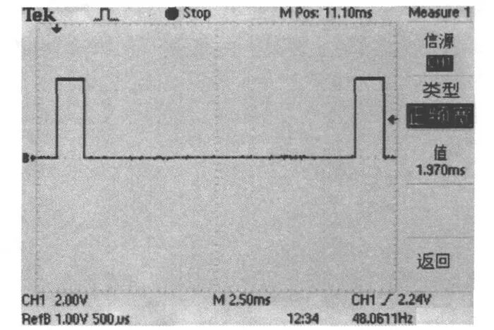 The implementation of serial port expansion is shown in Figure 3: ADR10 and ADR11 are the downlink address lines, where ADR10 and ADR11 = 00, 01, 10 correspond to sub-serial ports 0, 1, and 2 respectively; ADR00 and ADR01 are the uplink address lines, where ADR00 and ADR01 = 00, 01, 10 correspond to sub-serial ports 0, 1, and 2 respectively. The I/O ports of the F2812 are directly connected to the address lines of the SP2338. When sending data, the DSP changes the state of the I/O ports to alter the downlink address, selecting a specific sub-serial port; when receiving data, the DSP reads the state of the I/O ports to determine which sub-serial port the data is coming from, thus processing the received data accordingly. This improves system efficiency and reduces software consumption. RS232, RS422, and RS485 communication can be achieved through an external level conversion chip.2.3 Memory Expansion The F2812 includes 128K 16-bit FLASH memory. Considering capacity and speed, memory expansion is necessary for the system. A 64K word IS61LV6416 memory chip produced by ISSI is used as the program expansion memory. It operates at +3.3V power supply, with an access time not exceeding 12ns. No additional delay circuit is needed; its data and address lines are directly connected to the DSP’s data and address lines. The DSP’s pin 51 R/W is connected to the chip select signal CE of the IS61LV6416, and the DSP’s read and write select signals are connected to the read and write select signals of the IS61LV6416.2.4 PWM Signal Output The servos of the UAV’s actuators are controlled by PWM (Pulse Width Modulation) signals, utilizing changes in duty cycle. The multiple parallel PWM signals generated by the DSP, along with the signal isolation driving circuit for the servos, control the position of the servos to achieve the control objectives. The TMS320F2812 integrates a PWM control signal generator, with each event manager capable of producing 8 PWM outputs. Since the high level of the PWM output from the TMS320F2812 is +3.3V, while the servo control signal requires a high level of +5V for PWM signals, the PWM signals output from the DSP need to undergo level conversion to drive the servos. To prevent interference from the motor driver board to the main control board, a high-speed opto-isolator device 74LS245 is used to isolate the PWM signal, blocking the conducted interference from the motor driver board to the main control board.2.5 Reset and Power Circuit In the entire hardware design, the main DC power supplies used are +1.8V, +3.3V, +5V, and +12V. The onboard power supply uses TI’s TPS767D318, providing the required 1.8V voltage for the DSP and 3.3V voltage for the DSP and peripheral circuits through a 5V voltage regulator. All signals connected to the F2812 must consider level matching issues, which are resolved by using level shifting chips. The +12V DC power supply is provided by a battery, while other DC voltages can be obtained through a DC/DC conversion module. The +5V voltage is obtained through the integrated voltage regulator module LM7805. Considering that this system also requires 1.8V and 3.3V voltages, the LM1117 chip from IDT is used to perform level conversion on the 5V input voltage, allowing it to be reduced to 1.8V and 3.3V. The LM1117 provides current limiting and thermal protection. All power supplies on the target board can be provided by a single 5V voltage regulator module. Additionally, for debugging convenience, the system is provided with a manual reset by TI’s TPS3307. The reset signal is decoded by the CPLD and outputs two levels, high and low, resetting different components according to their reset level requirements. The manual button and all reset sources from the AT bus are introduced to the CPLD, which is processed by the built-in Reset Logic of the CPLD and then output to the reset destination.
3. System Software Design
The software system uses the embedded real-time operating system DSP/BIOs integrated in TI’s DSP integrated development tool CCS, employing a mixed programming approach of C language and assembly language. The system initialization module sets the working mode of the SJA1000, and its initialization can only be performed in reset mode. The initialization flowchart is shown in Figure 4.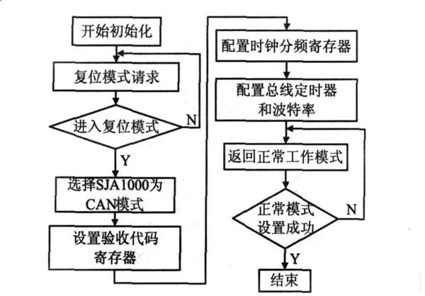 The system control flowchart is shown in Figure 5. Data storage is placed in the task thread, where the process involves storing the analysis results of flight data in FLASH. The detection task thread can be completed through the periodic function PRD. PRD can determine the function’s running time based on the real-time clock. Here, the detection task is set to run once every 100ms.
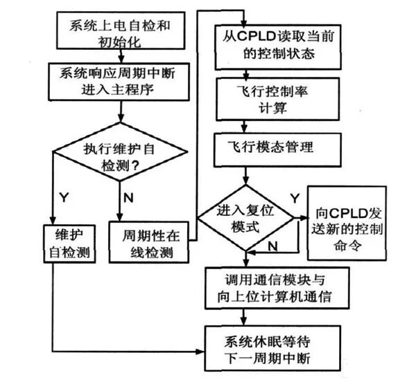 The startup of all tasks is closely related to the small cycle count on the flight control system bus, where tasks related to receiving bus data are initiated by the message dispatch thread. When the received message is the synchronization data code sent by PSP, the terminal synchronizes its small cycle count and starts the corresponding task according to the current small cycle. All tasks are included in the message processing thread, with each terminal having such a thread, allowing each thread to work independently, enabling parallel operation of each terminal. All logical control functions of the system are executed in a periodic manner, waking up every 10ms through the timer interrupt program. The CPLD is used for logical operations and data processing, detecting the analog input signal, determining the working status of each monitored object, and deciding the output based on the system control logic. When a status change occurs, it notifies the DSP to assist in completing the system’s self-detection function. In status monitoring, the currently detected status is compared with the previously stored status; if the two statuses are the same, no operation is performed; if a change occurs, an interrupt signal INT is sent to the DSP, notifying it to read the data. When receiving control commands sent by the DSP, the command is compared with the current status; if they match, no control command is sent again, thus preventing erroneous actions caused by multiple control command transmissions. During flight, the main tasks of the control system include collecting the UAV’s attitude data, calculating control quantities, and outputting them to servos and other actuators, as well as receiving commands from the ground station and transmitting the UAV’s position information. The designed control board is used to implement the servo control algorithm, completing the control of the actuator servos. Figure 6 shows the PWM control signal waveform output from one of the servos in the control system.
4. Conclusion
By utilizing the high-performance DSP chip TMS320F2812 combined with CPLD, and employing DSP/BIOS as the real-time operating system, a real-time multitasking design has been effectively implemented, significantly enhancing the system’s reliability and real-time performance. After debugging, the system has shown stable performance in actual operation, meeting the design requirements. This system is compact, lightweight, low-cost, and possesses certain scalability, making it suitable for constructing small UAVs with strong real-time capabilities, miniaturization, and low cost.
Recommended Reading

 1. A Brief Discussion on the Mavic Series UAVs and Their Compatible UAV Hangars;2 A Group of “Post-95s” from Huzhou Research Institute of Zhejiang University Overcomes World Problems in UAVs;3.Following the National Team, These Companies Also Appeared at the 2023 Abu Dhabi International Defense Exhibition;4.Analyzing the “Leverage Effect” of Unmanned Systems from Firefighting Practice;5.Vertical Takeoff and Landing Fixed-Wing UAV Airports, All Are Heavyweights;6. A Hundred Media Outlets Jointly Selected the “Top Ten Events in China’s UAV Industry in the Past Decade”, Joint Aircraft Stunned the Audience;7.The “Unmanned Aerial Vehicle Open Source and Application Exchange Conference” Successfully Held, Preley Company Supports the UAV Industry;
8.T900: A Domestic 900MHz Wireless Frequency Hopping Module That Perfectly Replaces P900;
9. The Ministry of Industry and Information Technology: Two International Standards in the UAV Field Led by China Have Been Officially Released;10.The 16th Security Expo Opened Grandly in Beijing, the First China Security Unmanned Systems Safety Summit Forum is Worth Looking Forward To;11.At the “First China Security Unmanned Systems Safety Summit Forum”, Interview with China Mobile (Chengdu) Industry Research Institute。