Click the “Beginner’s Guide to Vision” above, and choose to add “Star” or “Top“
Heavyweight content delivered first timeSource: Xilinx Authors: Aaron Behman, Adam Taylor
Based on vision, systems have become very common in many industries and application fields. In fact, many of us carry an embedded vision system every day, such as in our smartphones. These smart devices not only capture images and record videos but also execute augmented reality applications, showcasing how embedded vision technology has been widely accepted.
Improvements in processing power, memory density, and system integration have facilitated the growth of embedded vision in both traditional and emerging application areas (examples shown in Figure 1). This has also led to widespread acceptance of embedded vision in consumer, industrial, and governmental sectors, resulting in significant growth expected within the next decade. Table 1 lists some high-growth areas for embedded vision, some of which are obvious while others are less apparent.
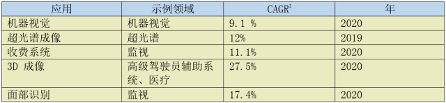
Figure 1 Common Embedded Vision Applications.
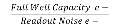
Table 1 Expected High-Growth Areas for Embedded Vision
What is Embedded Vision?
An embedded vision system encompasses the entire signal chain from receiving light from the selected imaging sensor to the system output. The system output refers to the processed or unprocessed images or information extracted from the images and provided to downstream systems. Of course, embedded system architects are responsible for ensuring end-to-end performance according to system requirements.
To this end, embedded vision system architects need to be familiar with various concepts and technologies related to sensors and post-processing systems. This article serves as a high-level introductory guide aimed at providing readers with a basic understanding of these technologies and concepts.
First, it is essential to be familiar with the electromagnetic spectrum and the spectral domain in which the system is expected to operate. The human eye can only see light in the spectral range from 390nm (blue light) to 700nm (red light), which is commonly referred to as the visible spectrum; imaging devices, depending on the technology used, can capture images across a broader range of wavelengths, including X-rays, ultraviolet, infrared, and visible spectrum.
In the near-infrared spectrum and below, we can use Charge-Coupled Devices (CCD) or CMOS (Complementary Metal-Oxide-Semiconductor) Image Sensors (CIS); when it comes to the infrared spectrum, specialized infrared detectors are required. The reason infrared spectrum requires specialized sensors is partly due to the excitation energy required by chip imagers (like CCD or CIS). These devices typically require 1eV of photon energy to excite an electron, while in the infrared range, photon energy ranges from 1.7eV to 1.24meV, thus infrared imagers should be based on HgCdTe or InSb. These devices require lower excitation energy and are often used with CMOS readout ICs (i.e., ROIC) to control and read out the sensor.
The two most common detector technologies are CCD and CIS.
● Charge-Coupled Devices are considered analog devices, so integrating them into digital systems requires using off-chip ADCs and clock generation functions under the required analog voltage levels. Each pixel stores charge generated by photons. In most cases, the pixels are arranged in a 2D array consisting of multiple rows, each containing multiple pixels. When reading out a CCD, each row is transferred in parallel to the readout register through row transfer, and then each row is serially read out through the readout register. During this register readout process, the charge is converted into voltage.
● CMOS image sensors allow for tighter integration, with ADCs, biasing, and driving circuitry all integrated on the same chip. This significantly reduces system integration requirements while increasing the complexity of CIS design. The core of CIS is the Active Pixel Sensor (APS), where each pixel contains both a photodiode and a readout amplifier, enabling CIS to read out any pixel address in the array, unlike CCD.
Although most embedded vision applications utilize CIS devices, CCDs are still used in high-end scientific applications that prioritize performance. The key points of this article apply to both imaging technologies.
Sensor Considerations
Selecting the right sensor requires an understanding of system requirements, which must be considered from several aspects of the device.
The first requirement is to determine the desired resolution, which is how many pixels per row and how many rows the detector needs. The ultimate application plays a decisive role in this, for example, astronomical applications for scientific research may require high-resolution 2D devices, while industrial inspection imaging may only need line scan solutions.
● Line scan devices contain a single row (sometimes a few rows) of pixels in the X direction. These devices are typically used to generate images in the Y direction through the movement of the camera or target. They are used in inspection or Optical Character Recognition (OCR) fields. Some areas require the use of Time Domain Integration (TDI) line scan sensors. These sensors contain multiple rows in the X direction, and as the target moves, pixel values move from one to the next, allowing for more sensitive detection as charges are integrated over time. However, TDI requires synchronization between row transfer and target movement to prevent blurring and image defects. Since only a few rows need to be read out, the frame rate can be very high.
● 2D arrays contain multiple rows, each with multiple pixels, and the array size is a factor in determining the maximum frame rate of the sensor. Typically, to achieve higher frame rates, 2D devices read out multiple pixels in parallel. 2D devices can also perform windowing operations (sometimes referred to as regions of interest), meaning they only read out specific areas of interest to achieve higher frame rates. Such devices can be used in numerous fields, with information contained in 2D images, such as Advanced Driver Assistance Systems (ADAS), surveillance, or scientific research.
After determining the imager format and required resolution, we must also consider pixel pitch. Pixel pitch defines the size of the pixels and determines how many incident photons can be collected to generate charge. Thus, smaller pixel pitch means less charge collected during the integration period (the time the sensor is exposed to the image). If the pixel pitch is too small, capturing images requires longer integration times, which affects the sensor’s ability to capture fast-moving images and reduces low-light photography performance.
After determining the sensor format, we must consider which technology to use, whether CCD, CMOS, or more specialized technologies. An important parameter here is Quantum Efficiency (QE), which is the efficiency with which the device converts photons into electrons. Typically, we want to achieve as high a QE as possible in the useful spectrum, which is also significant for low-light applications. Three factors affect the QE of the device: absorption, reflection, and transmission. One major reason for reduced QE is the device structure. The device structure may cause pixels to be shielded by circuits within the sensor, such as metal lines or polysilicon gate circuits. These structures can absorb or reflect photons, thus reducing QE, so it is crucial to select the right sensor.
● Front-illuminated — For this type of device, photons illuminate the device from the front in the traditional manner, which may shield the pixels, thereby reducing QE.
● Back-illuminated — These devices have been thinned from the back through post-processing to receive light from behind, thus unobstructed by other design elements. Thin back-illuminated devices can achieve optimal QE.
We must also consider the noise allowed in the image sensor; there are three main aspects to consider.
● Device noise — This is essentially temporary and includes shot noise and noise generated by output amplifiers and reset circuits.
● Fixed Pattern Noise (FPN) — This is spatially distributed and caused by different responses of pixels under the same illumination intensity. FPN is typically caused by different offsets and gain responses of each pixel; the offset part is commonly referred to as Dark Signal Non-Uniformity (DSNU), while the gain part is referred to as Photo Response Non-Uniformity (PRNU). There are various methods to compensate for FPN, with the most common being correlated double sampling of the output signal.
● Dark current — This is caused by thermal noise in the image sensor and can occur even in the absence of light. The impact of dark signals on the final image quality depends on the frame rate; at higher frame rates, the impact is minimal, but as the frame rate decreases (such as in scientific applications), the impact becomes significant. Since dark current is temperature-dependent, when it is necessary to reduce dark current, the common practice is to use cooling devices (such as Peltier) to lower the operating temperature of the imaging device.
Understanding the noise patterns of the imager allows us to determine the achievable Signal-to-Noise Ratio (SNR).
Once the noise performance of the device is determined, the required dynamic range of the image sensor can be established. The dynamic range represents the sensor’s ability to capture images over a wide range of illumination intensities, expressed in dB or in ratio form. This means the image contains both high-illuminance and dark areas.
The actual dynamic range of the sensor is determined by the full well capacity of the pixels, which is the number of electrons that can be held before the pixel saturates. Dividing this capacity by the readout noise provides an easy way to convert the ratio into a dB value.

Dynamic range is typically determined using photon transfer curve testing, which plots the relationship between noise and capacity.
If the device has a digital output, this value can be calculated using the number of output bits as follows.

However, this does not ensure that the device can achieve such dynamic range; it merely indicates the potential range represented by the bus width without considering sensor performance factors.
IO standards are also crucial, not only for outputting pixel data but also for outputting command and control interfaces. This is related to frame rates; for example, the LVCMOS interface is unsuitable for high frame rate applications but can be used for simple surveillance cameras. As frame rates, resolutions, and bits per pixel increase, imaging devices are trending towards utilizing LVDS series or SERDES technology for dedicated high-speed serial links.
Now that we have covered several important aspects of image sensors, another factor yet to be considered is whether the imager is a color or monochrome sensor. The choice depends on the application.
● Color sensors — These require a Bayer pattern on each pixel, alternating red and green on one line, and blue and green on the next line (green is used more because the human eye is more sensitive to green wavelengths). This means filtering the received photons so that each pixel only receives photons of the desired wavelength. We can post-process the image, surrounding each pixel with different colors to reconstruct the color of each pixel without reducing image resolution. Color sensors complicate the image processing chain required for reconstruction and output. The Bayer pattern does lead to a reduction in resolution, but not as much as imagined, typically around 20%.
● Monochrome — Since there is no Bayer pattern on the image array, each pixel can receive all photons. This increases image sensitivity and simplifies image readout since there is no demosaicing effect required for color reconstruction.
Having selected to use CIS devices, which are indeed complex specialized System on Chip (SoC), we must also consider the following issues regarding readout modes and integration times.
● Integration time — This is the exposure time of the pixels before readout. In simpler CCD systems, this timing needs to be executed externally to the device. However, for CIS devices, the integration time can be configured via command interface registers, allowing the CIS device to precisely execute the integration time for the two common readout modes.
● Global shutter mode — In this mode, all pixels are exposed to light simultaneously and then read out. This mode increases readout noise because all pixels are read out at the same time. It is suitable for capturing snapshots of fast-moving objects.
● Rolling shutter mode — In this mode, exposure and readout occur line by line. This mode has lower readout noise; however, it is not as effective as global shutter mode for capturing fast-moving objects.
System Development
Once the appropriate sensor is selected, there are many challenges to consider and address during the system development process.
In addition to technical challenges, there are also time pressures when developing systems, ensuring that products are brought to market within established timelines. We must clarify which parts of the development process can provide added value based on time constraints, making the right choices to distinguish which parts should be developed in-house (value-added activities) and which can be purchased as commercial off-the-shelf products (COTS) or outsourced. Focusing on value-added activities and utilizing IP modules at the hardware, software, and FPGA levels is one of the significant contributors to meeting time-to-market requirements.
In addition to time-to-market requirements, size, weight, power consumption, and cost (SWAP-C) requirements must also be considered during the development of embedded vision systems. Which requirements dominate depends on the specific application area; for example, handheld devices are more stringent regarding power consumption than driver assistance systems. However, for advanced driver assistance systems, the cost of the solution becomes the dominant factor due to the need to produce millions of units.
To achieve good results in size, weight, power consumption, and cost, tighter system integration should be implemented in the sensor and processing systems, utilizing fewer but more powerful integrated components.
Each application area has different value points and varying considerations for size, weight, power consumption, and cost, leading to the necessity for almost all embedded vision systems to implement what is known as an image processing pipeline. This pipeline can establish interface connections with the selected sensor and perform the required operations to generate images suitable for further processing or direct transmission over a network. A basic image processing pipeline includes:
● Camera interface — Receives raw images from the sensor
● Color filter array — Reconstructs pixel colors
● Color space conversion — Converts to the correct color space for the codec.
● Output formatting — Interfaces with the output medium
In the image processing pipeline, algorithms are applied to the received images. The specific algorithms implemented vary based on the application; however, there are several common image processing algorithms available to enhance contrast, detect features, objects, or motion in images, or correct blurred images.
These algorithms should be developed within a framework to allow us to bring products to market in the shortest possible time while encouraging reuse and minimizing non-recurring and recurring engineering costs. There are several off-the-shelf frameworks we can consider using.
● OpenVX — An open-source application for developing image processing applications.
● OpenCV — Open-source computer vision, multiple libraries aimed at real-time computer vision based on C/C++.
● OpenCL — An open-source computing language based on C++ for developing parallel processing applications common in devices like GPUs and FPGAs.
● SDSoC — Xilinx’s design environment that allows developers to initially implement algorithms written in C/C++ within the ARM processing system of Zynq or UltraScale+ MPSoC devices, analyze code base characteristics to identify performance bottlenecks, and then use Xilinx’s high-level synthesis capabilities to convert these bottlenecks into hardware-supported IP cores that run in the device’s programmable logic (PL) section.
When adopting FPGA or All Programmable SoC solutions, combining these frameworks with HLS enables efficient development of embedded vision applications and rapid demonstrations through hardware in a closed loop.
After the image has been processed through the pipeline, the method of outputting data from the system is also crucial; we have three options.
● Output images to a display using standards such as Video Graphics Array (VGA), High-Definition Multimedia Interface (HDMI), Serial Digital Interface (SDI), or DisplayPort. Many electric vehicles use touchscreen displays to control and configure the system.
● Transfer images or extracted information from the images to another system that uses the images or extracted information, such as cloud processing applications.
● Store images in non-volatile storage media for later access.
For the vast majority of methods, after completing the imaging chain, we need to determine how to format the images for use. At this point, we need to decide whether to use industry-standard image/video compression algorithms such as H.264 (MPEG-4 Part 10 Advanced Video Coding) or H.265 (High Efficiency Video Coding) to encode the images; these implementations are commonly referred to as codecs. Codecs can improve the efficiency of communication and network bandwidth usage or reduce the storage space required for high fidelity, as encoding often incurs significant distortion. If the distortion caused by using a codec is unacceptable, images can also be sent and stored in their original format or encoded in a lossless format.
Most codecs use a color space that differs from the color space output by the image sensor (assuming the system uses color devices). Common color spaces in embedded vision include:
● Red, Green, Blue — Contains RGB information as the output of the image sensor, commonly used for outputs such as VGA.
● YUV — Contains luminance (Y) and chrominance (U and V), this color space is used for most codecs and some display standards. Common YUV formats include YUV4:4:4 and YUV4:2:2. The difference between the two formats is that in the 4:4:4 format, each pixel is represented by 8 bits, resulting in 24 bits per pixel. In the 4:2:2 format, U and V values are shared between pixels, resulting in 16 bits per pixel, saving storage space.
Another decision that significantly impacts the image processing chain and SWAP-C is where most of the image processing chain should be implemented:
● At the edge, that is, within the embedded vision system. This will increase the system’s power consumption and processing/storage requirements but enables faster response times. Edge processing will become dominant in most embedded applications (e.g., advanced driver assistance, machine vision, etc.).
● In the cloud, this requires the embedded vision system to capture images and use network technology to send the images to the cloud. Typical applications that can be processed in the cloud include medical imaging or scientific applications. In these applications, processing is very intensive and does not require real-time results.
To implement the processing chain, the processing core at the heart of the embedded vision system must not only control the selected image sensor but also receive and implement the image processing pipeline and transmit images via specified network infrastructure or send them to selected displays. Given these stringent requirements, it is often necessary to select FPGAs, or increasingly, All Programmable System on Chip solutions like Zynq devices.
Zynq devices combine two high-performance ARM A9 processors with FPGA architecture. This allows the processing system (PS) to communicate with the host system via interfaces such as GigE, PCIe, or CAN while executing general management and daily tasks of the system. The other half of the device, the programmable logic (PL), can receive and process images, fully leveraging the parallel processing capabilities of the FPGA architecture. If images need to be transmitted via network infrastructure, the DMA controller in Zynq can efficiently move image data from PL to PS DDR memory. Once the image is in PS DDR memory, it can be further accessed using the DMA controller of the selected transmission medium.
Of course, once the image is in PS DDR, the high-performance A9 processors can also provide further processing operations. The Zynq architecture’s feature is that it can also move the processed images back from PS DDR to the image pipeline in PL.
Sensor Fusion
Many embedded vision systems also require the ability to integrate more sensor data for better environmental perception. This includes using many similar sensors (homogeneous sensor fusion) to expand the field of view, such as panoramic functions in advanced driver assistance systems; or integrating multiple different types of sensors (heterogeneous sensor fusion) to provide visual content not visible in the visible spectrum, such as overlaying infrared information on conventional image sensor data.
In many cases, it is necessary to fuse the outputs of embedded vision applications with data from other sensors, resulting in images containing information from multiple different sensors. The simplest sensor fusion application is combining images from different spectra, such as visible light and infrared fusion to achieve better night vision.
A more complex use of sensor fusion is to integrate imaging systems, Global Navigation Satellite Systems (GNSS), digital map information, and other sensors operating at different wavelengths (e.g., radar) to determine the relative position of another vehicle, enabling collision avoidance functions.
Due to the need to integrate different systems and extract information, sensor fusion places very high demands on processors. All Programmable SoC solutions can interface with multiple sensors, process information in parallel, and significantly increase data throughput, thus offering multiple significant advantages.
Conclusion
Embedded vision has become very common, and its market penetration and application scope will only increase in the next decade.
At both the sensor and system levels, there are multiple factors to consider. There are various technologies, frameworks, and devices available to implement embedded vision systems.
Good News!
The Beginner’s Guide to Vision Knowledge Planet
Is now open to the public👇👇👇
Download 1: OpenCV-Contrib Extension Module Chinese Tutorial
Reply "Extension Module Chinese Tutorial" in the "Beginner's Guide to Vision" public account backend to download the first OpenCV extension module tutorial in Chinese, covering installation of extension modules, SFM algorithms, stereo vision, target tracking, biological vision, super-resolution processing, and more than twenty chapters of content.

Download 2: Python Vision Practical Project 52 Lectures
Reply "Python Vision Practical Project" in the "Beginner's Guide to Vision" public account backend to download 31 vision practical projects including image segmentation, mask detection, lane line detection, vehicle counting, eyeliner addition, license plate recognition, character recognition, emotion detection, text content extraction, face recognition, etc., to assist in rapidly learning computer vision.

Download 3: OpenCV Practical Project 20 Lectures
Reply "OpenCV Practical Project 20 Lectures" in the "Beginner's Guide to Vision" public account backend to download 20 practical projects based on OpenCV for advancing OpenCV learning.

Group Chat

Welcome to join the public account reader group to exchange with peers; currently, there are WeChat groups for SLAM, 3D vision, sensors, autonomous driving, computational photography, detection, segmentation, recognition, medical imaging, GAN, algorithm competitions, etc. (will gradually be subdivided later). Please scan the WeChat number below to join the group, and note: "Nickname + School/Company + Research Direction", for example: "Zhang San + Shanghai Jiao Tong University + Vision SLAM". Please follow the format; otherwise, you will not be approved. After successful addition, you will be invited to enter the relevant WeChat group based on your research direction. Please do not send advertisements in the group; otherwise, you will be removed from the group. Thank you for your understanding~