This article is reprinted from the Extreme Community.
Extreme Column: ARM Chip Building Guide
Author: djygrdzh
After a year, I finally have the chance to build a chip again. This time, it’s the hot automotive chip.
I remember two years ago, there were hardly any companies in China making pre-installed automotive chips. Fast forward two years, and suddenly more than ten companies have sprung up, covering areas such as assisted driving, central control, dashboard, T-Box, gateway, body control, battery management, hardware encryption and decryption, LiDAR, millimeter-wave radar, image sensors, and image signal processors, each showcasing their unique capabilities.
Globally, the annual sales of automotive chips is roughly $40 billion, with digital chips accounting for $10 billion: infotainment (central control) chips about $2.5 billion, averaging $25 each; MCUs around $6 billion, 300 million units, averaging $2; assisted driving about $1.7 billion. Approximately 100 million vehicles are sold globally each year, with an average of $100 worth of digital chips per vehicle. The assisted driving chip segment is experiencing rapid growth. Major suppliers of automotive chips include NXP, Renesas (with more digital components), Infineon, and Texas Instruments (more analog components). Automotive chips are one of the few remaining markets with decent profits; the technological barriers are not insurmountable, and there is no absolute ecological closed loop. However, the volume is not as large as consumer electronics, with only a few million units produced annually being considered good. In this field, new car manufacturers are emerging, while traditional manufacturers pursue differentiation, coinciding with the hotspots of 5G, autonomous driving, and artificial intelligence, making automotive chips a new investment direction following virtual reality, mining machines, NB-IoT, and artificial intelligence.
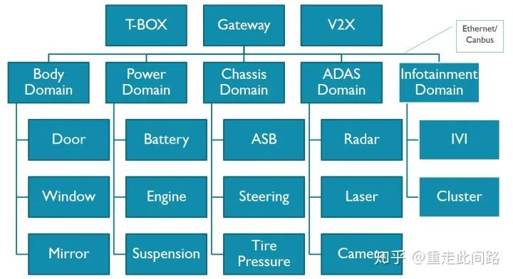
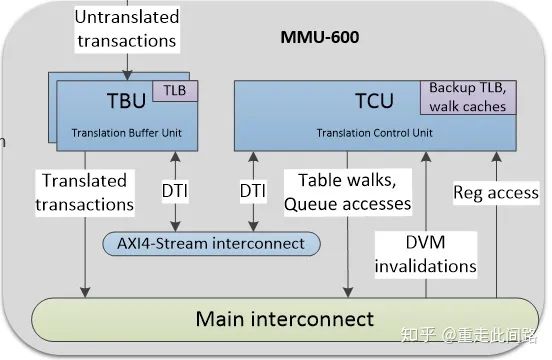
The above image shows a typical automotive electronic system framework. This system is divided into several domains: body, powertrain, chassis, infotainment, assisted driving, gateway, and T-Box. Each domain has its own domain controller, interconnected via in-vehicle Ethernet and CAN bus. Let’s take the most complex central control and assisted driving chips as examples to discuss their design ideas and methods.
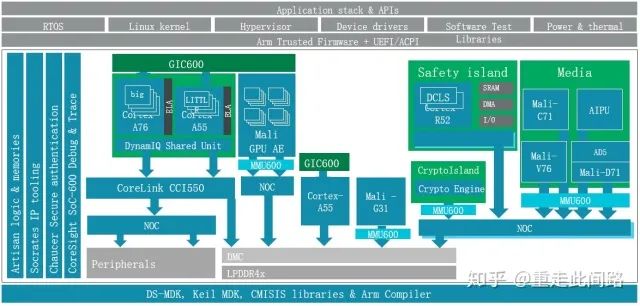
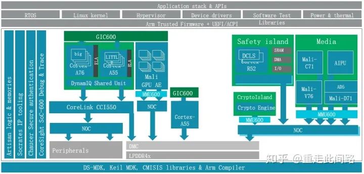
The architecture of the new generation of central control chips is as shown in the figure below, mainly consisting of subsystems such as processors, graphics processors, multimedia, image processing, security management, functional safety, on-chip debugging, and bus. The main difference from conventional application processors lies in virtualization, functional safety, real-time performance, and automotive-grade electrical standards.
First, let’s talk about virtualization. Virtualization is a concept that originated from servers; why would automotive systems also require it? There are two reasons: currently, there is a trend in central control chips to integrate instrument panels to reduce costs. Previously, instrument panels were typically made using microcontrollers with relatively simple graphic interfaces. Now, systems are becoming more sophisticated and may even require graphics processors to participate. Naturally, this leads to the integration of central control and instrument panels into a single chip. They run different operating systems, and virtualization can better achieve software isolation. Of course, some manufacturers believe that virtualization is not enough and require physical isolation for security, but that’s a topic for later discussion.
The hardware requirements for virtualization are not clearly defined. It can rely on the processor’s built-in second-level memory management unit (s2MMU) to implement software virtual machines; a hardware firewall MPU can be placed before the memory controller to check and filter memory access addresses without address remapping; or a system memory management unit (SMMU) can be used to implement complete hardware virtualization, which we will focus on introducing.
As shown in the yellow box in the figure above, an SMMU600 is added between each master device and bus. Why is it necessary to add one after each master device? The reason is simple; if not added, there will inevitably be security vulnerabilities, making software virtualization no different. Why not use an MPU? The implementation method of MPU typically uses an on-chip memory to store filter table entries. If a granularity of 4K bytes is achieved, then a 4G byte memory would require 1 million entries, each 8 bits, totaling 1MB of on-chip memory, which is a significant cost. Another reason is that the physical address space of the MPU scheme is opaque to software; using SMMU is transparent to upper-layer software, which is closer to the needs of virtualization.
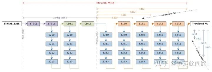
When the processor initiates a virtual-to-physical address translation request, the MMU will look for the final page table entries and intermediate table entries in the internal TLB cache and Table Walk cache. If not found in the internal cache, it will need to read from the system cache or memory. In the worst-case scenario, every level of the four-layer intermediate table may miss, requiring 20 memory reads. For SMMU, the situation may be worse. As shown in the figure above, because SMMU itself also needs to introduce multi-level descriptors to map multiple page tables, in the most extreme case, it may require up to 36 memory accesses to find the final page table entry. If all accesses incur this delay, it is clearly unacceptable.
Arm’s traditional design adds sufficiently large multi-level TLB and Table Walk caches, resulting in the following performance:
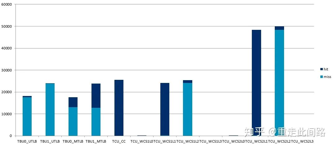
This is the measured result after enabling 2-stage address mapping, with each cache size configured to be quite large, and then connecting two master devices to the interface for relatively random address access. It can be seen that the 50,000 accesses from the master device, after passing through the SMMU, resulted in nearly 50,000 misses. This means that the average access delay equals the memory access delay, which is over 150ns. On the other hand, after enabling virtualization, the random memory access efficiency of the processor can achieve over 80% compared to when virtualization was not enabled. Why is that? The answer is simple: the internal MMU of the processor will continue to send the physical addresses of the intermediate page tables to the second or third-level cache, utilizing the cache to reduce average latency. However, SMMU is not so lucky; in Arm’s previous mobile processor reference design, there was no system cache. In this case, even for master devices that are not sensitive to latency, such as graphics processors, enabling virtualization can still cause performance loss of up to 9%, which is not insignificant.
How to solve this problem? In Arm’s server and next-generation mobile chip reference designs, a mesh structure bus will be introduced instead of the previous crossbar structure for cache coherence. The advantage of the mesh structure bus is that it enhances frequency and bandwidth, and while providing multi-core coherence, it can also allow system caches to be utilized by various master devices. Master devices that do not require caching can still perform non-cached data transfers as before, avoiding additional cache usage and frequent cache replacements; at the same time, SMMU can place page tables and intermediate page table entries in the cache, thereby shortening latency.
Arm’s SMMU600 has also made some improvements, allowing TLB caches to be placed close to various master devices. In the event of a hit, translation can be completed in one clock cycle; at the same time, the Table Walk cache is placed elsewhere, and the TLB cache and Table Walk cache are interconnected via an internal bus. Several master devices can simultaneously use a single Table Walk cache, reducing area and easing wiring while maintaining efficiency. Its structure is as follows:
If we read Arm’s SMMU3.x protocol, we find that it supports bidirectional page table maintenance information broadcasting, which means that apart from cache data consistency, all master devices can share a single page table as long as they comply with the SMMU3.x protocol. In the design of assisted driving chips, if necessary, important accelerators can be added to the same page table to avoid software page table update operations, further improving the efficiency of heterogeneous computing. However, as for SMMU600, it only supports unidirectional broadcasting; master devices connected to SMMU600 cannot broadcast their own cache and page table operations to the processor, although the reverse is possible.
For current automotive chips, if there is no system cache, how can we reduce the virtualization latency of devices? There are also ways to achieve this. The virtual machine applications in automobiles are quite special; currently, eight virtual machines are sufficient to handle all split-screen and multi-system needs, and once allocated, there is no need to repeatedly delete and generate during the operating phase. We can fully utilize this point to enlarge the second-stage SMMU page table, for example, assigning 1GB fixed to a certain virtual machine. In this way, when the device performs two-stage address mapping, it only needs a few TLB entries to achieve continuous hits, greatly reducing latency. It should be noted that once the physical space of the second-stage mapping is assigned to a certain device, it cannot be reclaimed and reassigned to other devices. Otherwise, after multiple recoveries, physical address fragmentation will occur, making it impossible to find continuous large physical addresses.
SMMU accepts physical addresses sent from the master device; how does it distinguish between virtual machines? It relies on vmid/streamid sent from the master device. If the master device itself does not support virtualization, it needs to be time-division multiplexed, allowing software to write vmid/streamid. Of course, this software must run in the hypervisor or secure monitor; otherwise, there will be security vulnerabilities. The specific approach is that when switching virtual machines, the hypervisor modifies the register-based vmid/streamid and provides input to the SMMU. If the id during access does not match the preset one, the SMMU will report an exception to the hypervisor.
If the master device wants to implement hardware support for virtualization, it needs to actively send different vmid/streamid based on multiple sets of register settings. For software compatibility, different sets can be separated by 4KB boundaries, allowing the same physical address to access different sets of registers during two-stage address mapping, while remaining transparent to the driver. Meanwhile, internal resources must also be differentiated to prevent data from interfering with each other. If caching is used, the cache must also be vmid-sensitive, identifying hits as misses for the same address but different vmids.
If the master device itself does not support virtualization and is particularly complex, then a custom driver is required. Taking Arm’s graphics processor as an example, so far, hardware has not formally supported virtualization; if software is to support it, there may be the following solutions:
Assuming we are using Hypervisor Xen, which runs on Arm processors at EL2 and virtual machines run at EL0/1. Normally, the graphics processor driver is divided into user space and kernel space. To achieve virtualization, the graphics processor must be time-division multiplexed; Xen cannot run the driver itself because the current driver only supports Linux. Therefore, the virtual machine can only run the original driver, and there is no way to run another driver on the hypervisor to perform access control. At the same time, remapping the graphics processor’s two-stage address on the CPU allows register access and data paths to be in ‘bypass’ mode without causing exceptions, improving efficiency. Correspondingly, allowing the virtual machine to directly access registers means that access control cannot be implemented. To schedule multiple virtual machines, we can implement a scheduler within the hypervisor and open interfaces in the kernel driver part, allowing the hypervisor to proactively schedule. The schematic is as follows:
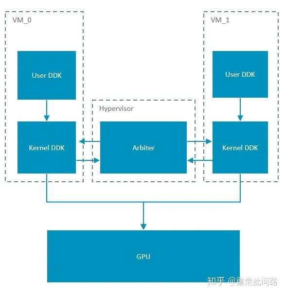
The advantages of this implementation are obvious: it requires less modification and is simple to implement, adaptable to both Xen and KVM. The downside is that the initiative is not in the hands of the hypervisor; if a rendering task on a certain virtual machine is too heavy and does not relinquish control to the scheduler, it will have to be forcibly restarted. Another obvious drawback is that it is not possible to run tasks from two virtual machines simultaneously on the graphics processor. This requires another implementation method for virtual machines, as shown in the figure below:
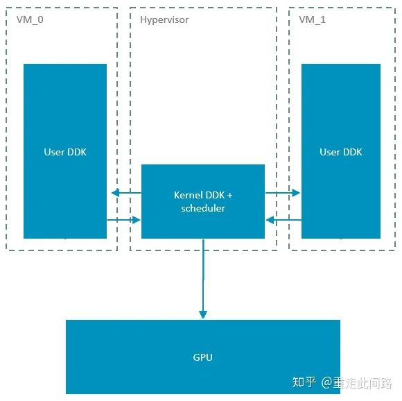
In this implementation, only the user space running the driver is in the virtual machine, and all calls involving kernel space are thrown to the hypervisor. This requires the hypervisor itself to be Linux, and only KVM meets this requirement. Arm’s Mali graphics processor, in hardware, supports specifying a certain rendering core to run specific tasks, meaning that a task from a certain virtual machine can be run on a specific rendering core. Thus, if a real-time operating system needs to run, such as a dashboard, a core can be reserved to avoid being occupied by other virtual machines, achieving a certain degree of QoS. At this point, the graphics processor can truly run tasks from two virtual machines simultaneously, rather than time-division multiplexing. As for the output frame buffer, different tasks can be placed at different physical addresses, but it cannot distinguish between StreamIDs, hence cannot achieve isolation.
It is estimated that Arm’s graphics processors that support hardware virtualization will not be available for another year. In terms of specifics, virtualization requires not only grouped registers and cache sensitivity to vmid, but also that some general units need to support grouping.
Regarding the efficiency of virtual machines, there are two more points that need to be noted:
The existing interrupt controller GIC600 is limited by the GICv3.x protocol and cannot bypass the hypervisor to directly send virtual interrupts to the Guest OS. External interrupts must still go through the hypervisor’s permission setting registers, generating a virtual interrupt to the Guest OS. Directly sending interrupts to the Guest OS will be improved in GICv4.
Armv8.1 and later CPUs support a mechanism called VHE, which can accelerate the switching of type 2 virtual machines. The specific principle is that for type 2 virtual machines like KVM, the hypervisor runs within the Linux kernel, while Linux requires a complete two-stage three/four-layer page table. On the other hand, processors prior to Armv8.1 did not have corresponding page tables for EL2. Without VHE, the hypervisor must keep some parts resident in EL2 for high-privilege operations, while the Host Linux still runs in EL1. This means that many operations require transitioning from EL1 to EL2, making modifications and then returning to the EL1 Linux kernel, adding an extra layer of jump. With VHE, the Host Linux kernel runs directly in EL2, allowing it to manipulate the page table registers of the four-layer page tables in EL1 without needing software modifications. On the hardware side, these accesses will be redirected to EL2 to ensure privileges.
For type 1 virtual machines, such as Xen, this change has no impact. Here we should mention the QNX virtual machine, which is a type 1 virtual machine. QNX is currently the only operating system that can reach the Asil-D level (including the hypervisor). If an Asil-D level system is to be implemented, existing software must be ported from the Linux system to QNX. Fortunately, QNX also complies with the Posix standard, especially for graphics processor drivers, making the migration process easier. Not all modules in QNX are Asil-D level, and the drivers migrated over do not actually have a safety level. QNX relies on Asil-D level core software modules and hypervisors to guarantee over 99% fault coverage. If a sub-module encounters an issue, it can only restart the sub-module.
It was previously mentioned that some manufacturers believe that virtualization is not enough; some scenarios require physical isolation. In virtualization, hardware resources are still shared, only transparently to software. This does not completely prevent hardware conflicts or guarantee priority. Please note that hardware isolation is Separation, not Partition; Partition is done using MPU. In the central control system framework diagram, the parts using physical isolation are highlighted in red, as shown in the figure below:

At this point, processor A55 and graphics processor G31 are independent of processor A76/A55 and graphics processor G76 serving as the infotainment domain, each having its own power supply, clock, and voltage. As an optimization, the red part can be connected to the remaining processors using a coherent bus, allowing it to be used as part of SMP when not serving as an instrument panel application. When isolation is needed, it can be connected to NoC or memory controller via a multiplexer. This saves area while achieving isolation.
Similarly, the graphics processor also has physical isolation requirements. The implementation is not complicated and is more straightforward than supporting hardware virtualization, as shown in the figure below:
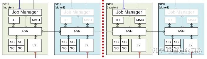
As the graphics processor’s largest area is the rendering core SC, this part remains unchanged. The other hardware modules each replicate a copy, and groups are interconnected via an internal bus ASN. When split into multiple graphics processors, each redundant module controls its own resources. At this point, each group of GPUs needs to run a driver independently. When all resources are merged, the redundant parts automatically shut down, and one module centrally schedules. At this point, certain shared resources may encounter performance bottlenecks, but automotive applications typically only require physical isolation of two groups, one for the dashboard and one for infotainment. The dashboard requires fewer resources, and during merging, the shared units of infotainment can be enabled to avoid bottlenecks. Similar design ideas can be applied to achieve isolation for other master devices in the system.
With graphics processors that support both virtualization and hardware isolation, our central control chip architecture will undergo the following changes:
At this point, the physical isolation of the graphics processor and hardware virtualization can be enabled simultaneously, allowing multiple drivers to run, meeting the requirements mentioned earlier.
Thus, we conclude the discussion on virtualization and isolation, and begin discussing automotive standards.
Currently, when we talk about automotive standards, we refer to two aspects: functional safety and electrical standards. The former is defined by ISO26262, while the latter is defined by AEC-Q100.
The design principle of functional safety on chips is to identify and correct as many failure scenarios on the chip as possible. Failures can be categorized into systematic and random types; the former is guaranteed through design process specifications, while the latter relies on various failure detection mechanisms implemented in chip design. Here, we mainly discuss the latter.
In simple terms, the failure rate of a chip is derived from the failure probability of a single transistor at a certain process node, resulting in the failure probability of on-chip logic or memory. The larger the area and the more transistors, the higher the corresponding failure rate. ISO26262 categorizes safety levels, commonly seen as ASIL-B and ASIL-D levels. ASIL-B requires the chip to cover 90% of single-point failure scenarios, while ASIL-D requires 99%. This is indeed a very high requirement. Although the failure probability of a single transistor is low, a complex chip usually consists of hundreds of millions of transistors; without any measures, any minor error could lead to functional failure, resulting in a high failure rate.
Appendix D of the fifth part of the ISO26262 manual provides detailed descriptions of hardware failure detection methods. In this section, the hardware system is divided into several modules: input components such as sensors, connectors, relays, and digital-analog interfaces; processing parts include processing units and various types of memory flash storage. The system level includes buses, power supplies, and clocks. The system framework is as shown in the figure below:
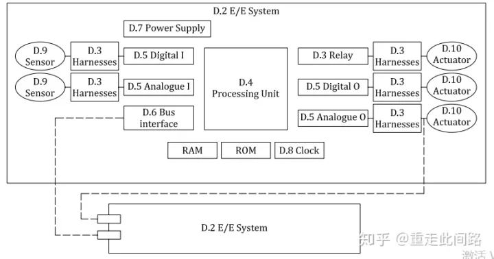
For each unit, the ISO26262 manual defines methods to detect whether these units have failed and provides the reliability of each method. For instance, transmission lines can use checksums, timeouts, counters, and sending test vectors, etc. For processing units, methods such as software and hardware self-checks, redundancy and comparison, and additional hardware module monitoring can be employed. These methods cannot be simply applied to chip functional safety design. So how to address this on chips? We adopt a bottom-up approach, starting from transistor analysis, then to IP module level, and finally to chip system level, discussing several typical scenarios, before performing a top-down analysis.
In the random errors on chips, there is a type of permanent error, such as a logic or on-chip memory bit stuck at 0 or 1, or simply short-circuited or open-circuited. For this type of error, during chip packaging and testing, we can use boundary scan and MBIST to discover defective transistors. Thus, the problem becomes how to improve the coverage of DFT. The industry already has mature methods for this.
Having factory testing is not enough; transistors will gradually age and fail during use. Therefore, we need to perform self-checks every time the system starts up to detect problems early and reduce the likelihood of errors occurring during system operation. At this point, we need to use LBIST and MBIST. Their principle is similar to that of factory testing, also utilizing scan chains; however, the chip needs an LBIST/MBIST controller to run test vectors and templates. Naturally, this will introduce additional costs. The higher the coverage, the greater the cost.
Even with LBIST/MBIST, it is still not sufficient; we need to detect errors within a few clock cycles after a transistor fails, not just at startup. For logic, the most direct method to achieve this is to use redundancy design, which means duplicating the logic and then using hardware comparators to compare outputs. This is usually referred to as lock-step design. Theoretically, for finite state machines, as long as the inputs and clock cycles are consistent, the outputs should also be consistent. Typically, digital components do not have truly random units; even cache replacement algorithms are pseudo-random, so the above conditions can be satisfied. The result of redundancy is that the logic area doubles, and the comparator will also introduce some additional area overhead and timing impacts.
Is it that simple to achieve functional safety? It is not; several issues need to be resolved:
The first issue is what the comparator actually compares. Taking processors as an example, if we only add comparators at the bus interfaces, many internal modules of the chip, such as write buffers, cannot pass the influence to the external interface within a short and definite time, which could lead to the processor being in a failure state without being detected. In this case, we cannot claim that the current redundancy mechanism can cover this type of failure. To address this, we need to connect the comparators to the internal submodule interfaces and analyze whether the impact can be seen in a short time. This needs to be considered during the design phase, and the specific approach is shown in the figure below:
For any register, it is possible to find the combinational logic and the upper-level register that influences it. If any point on this path fails, we can see an inconsistency between the output of the register and that of its redundant module after one clock cycle. We record this node as 1, and then take the input register of 1 as the new starting point to find node 2. By repeating this process, we can find a non-circular path, and any point on this path can reflect a problem within a determined short time. We call this path module X. With the help of certain EDA tools, we can identify several modules X within the chip, as shown in the example below:
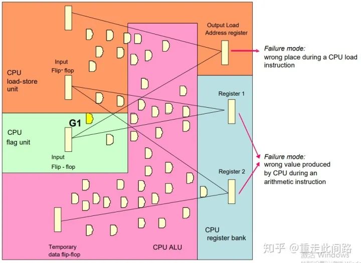
Here, the IP module is divided into access units (A gates), flag units (B gates), computation units (C gates), and register groups (D gates). From the output end, the combinational logic covered by connections to the previous-level registers is counted as gates, with one register counting as ten gates. As shown in the figure, the access unit’s address register output is influenced by 24 combinational logic gates plus 2 registers, resulting in 44 types of single-point errors that could cause failure. Similarly, the output of register group 1 is influenced by 28 gates, while that of register group 2 is influenced by 49 gates. In total, there are 121 possible failures. A simple calculation shows that the failure rate of the access unit is 44/121=36.4%, while the combinational logic of the register sums to 77/121=63.6%. Some gates, such as G1 in the figure, are counted multiple times, which will reflect in the total probability.
Based on the above ideas, let’s see how processors handle this. With the help of EDA tools, we divide them into several major modules: memory management units, write buffers, instruction-fetch units, data processing units, program trace buffers, data/instruction caches, bus interface units, clock and reset control units, ECC/parity control units, interrupt interfaces, and monitoring control units. Here, we do not include on-chip memory; even when discussing caches, we are referring to the control logic part.
Within each unit, it can be further subdivided into many submodules. Taking the data processing unit as an example, it can be further divided into general register groups, access units, floating-point units, floating-point register groups, decoding units, debugging units, control signal units, system register groups, branch execution units, etc. Each subunit can be subdivided again. The purpose of this subdivision is to determine whether the registers influenced by the transistor failure will fail, and whether this failure can be detected by external comparators. This requires bringing internal signals to the outside. So how do we decide which signals to pull out and which not? Is the coverage sufficient? The nodes and module information provided by the tools can only serve as a reference; designers still need to check each one to make the final decision. Typically, many signals are pulled out; for example, in Cortex-R5, out of over 200,000 gates of logic, the number of signals sent to comparators reaches over 2,000, averaging one signal per 100 gates.
During chip certification, if the IP itself has not been certified or has not been widely used before, the certification agency may need to discuss each pin with the chip company to see whether the connected pins provide sufficient failure detection coverage. Typically, this design-related information is not provided by IP companies to chip companies, so the certification company may need to obtain this information from the IP design company, resulting in longer certification time. Conversely, if it is a widely used IP module, this time can be shortened.
Having solved the coverage issue of redundancy design, there is a second issue. If subjected to electromagnetic interference or radiation, even with redundancy design, both modules may fail simultaneously. This is relatively easy to handle; simply staggering the inputs of the two identical logics by a few clock cycles will suffice. When outputting, stagger the same number of cycles so that the comparator still sees the same result.
The third issue is that if a logic comparator identifies an error, can it correct it? Unfortunately, it cannot. Unless two identical logics are duplicated, with three comparisons, this would increase the area of the original logic by 100%. For large processor designs, no one typically does this. If it is a small logic such as a watchdog circuit, this is feasible.
The fourth issue is that the logic comparator itself may also fail. This type of error is defined by ISO26262 as a latent fault. If the coverage rate of the comparator itself is found to be insufficient, redundancy design can also be applied to the comparator to improve its coverage. For ASIL-D, the latent fault coverage rate needs to reach 90%, while for ASIL-B, it is 60%.
All the above analyses pertain to logic errors. There is also a type of error related to memory. Here, memory refers to on-chip memory, including embedded flash memory. Memory errors are relatively easy to detect; typically, ECC can achieve a 99% coverage rate, correcting one bit while reporting multiple errors. Some memories, such as level one instruction caches, only support parity checks and do not support corrections.
For logic redundancy and memory ECC, error injection mechanisms need to be integrated into the chip. Please note that the error injection mechanism is not for verifying single-point and multi-point error failure rates but for verifying whether the error detection mechanisms themselves can meet design requirements.
In summary, logic redundancy and memory ECC are necessary means to help us achieve ASIL-B/D levels. When there is no redundancy design, running a program twice on one core and then comparing the results is also a way to achieve high-level safety, but this only applies to simple, non-time-sensitive computations. If there are permanent errors, this method will fail and require continuous online detection. Likewise, using two non-redundant processors to perform the same computation simultaneously is also a method. However, if the computation is complex, this will not only increase system latency and bandwidth but also incur significant costs. These two methods cannot fundamentally improve safety levels; if the final safety level requires ASIL-D, the aforementioned methods will require that the decomposed submodules also reach ASIL-B. Moreover, achieving ASIL-B’s single-point 90% coverage rate is also difficult without redundancy mechanisms. Another method is to perform single-path calculations while judging whether the result is reasonable. This monitoring path can be raised to ASIL-D. This is only possible in specific scenarios, which we will discuss later. Therefore, to achieve general ASIL-B/D, it is best to start using logic redundancy and memory ECC from the design stage.
In actual design, especially for processors, there is a set of error detection and correction mechanisms in addition to redundancy design. Arm refers to it as RAS (Reliability, Availability, Serviceability). RAS cannot replace redundancy design to achieve ASIL-B/D, as its coverage rate is too low. However, in some scenarios, such as ECC errors and instruction errors, this mechanism can correct errors without restarting the core or prevent errors from spreading (Data Poisoning), or record the context of errors. This is its advantage and has some utility in chips without redundancy design.
Let’s combine the ISO26262 document to see how Arm’s automotive application IP achieves high-level functional safety.
The above is the A76AE configuration diagram, which is aimed at automotive applications. It introduces the Split-Lock design. Under normal circumstances, it can be used as 4-core SMP, while in redundancy mode, all logic and memory within the core are duplicated, serving as backups. Switching between these two modes requires a restart, which is sufficient for automotive applications. The comparators added internally account for about 5% of the area, and there will be about a 5% loss in frequency.
The new A76AE is based on the Armv8.2 architecture, as shown in the figure above. Within a processor group, it includes a DSU for level-three cache and internal interconnects. Unlike the core part, a traditional lock-step mode is used here, only duplicating logic while retaining a single memory. This saves considerable area overhead for the cache. Typically, the logic within the DSU occupies a small portion, and the area utilization is low, so the additional area is not significant, about 15%.
Arm also has a processor A65AE that supports automotive ASIL-D levels, which can serve as a small core placed in different processor groups and interconnected with large cores via the CMN600AE bus, providing high energy efficiency for heterogeneous computing. A65AE supports single-core dual-threading by adding a register group, allowing two software threads to share the pipeline on a single physical core, remaining transparent to software. This actually originated from the needs of network processors, where execution units often wait for high-latency read transfers. To enhance pipeline utilization, A65AE adds about 5% more hardware registers, improving total performance by about 20%.
The following image shows the various combinations of A76AE and A65AE in assisted driving chips. In automotive applications, especially in assisted driving, there are scenarios where both large and small cores are needed: large cores handle decision-making with high single-thread performance; small cores handle computations with high energy efficiency.
Next, let’s take a look at the safety design issues of the media section. The above image shows the rearview subsystem, where the image signal processing is handled by C71 (ASIL-B), R52 (ASIL-D), bus NIC450 (QM), DMA330 (QM), SRAM (with ECC), and display module D71 (QM). The subsystem requires achieving ASIL-B levels. Since not all modules have reached ASIL-B, we need to perform failure tree analysis. The real failure scenarios occur when the display freezes on a certain frame. Instantaneous errors, such as a bad pixel in a frame, do not constitute a failure. Therefore, our tasks become twofold: first, use R52 to obtain the CRC of each frame from the display module, checking if multiple consecutive frames remain unchanged; if an error is detected, an alert should be triggered immediately, and this calculation must be completed within the failure tolerance time interval; secondly, periodically run LBIST/MBIST to check for permanent errors, which also need to be alerted. As long as the source of the image, C71, has ASIL-B and R52 is higher than ASIL-B, we can relax the requirements for detecting instantaneous errors in the other modules.
Next, let’s look at the framework of the assisted driving chip. Unlike central control, assisted driving requires perception and decision-making, which is a complex real-time computation process. It cannot achieve high-level safety simply through monitoring by the safety island; it must be ensured by the processors themselves. Therefore, all processors here are replaced with A76AE and A65AE with redundancy design. Virtualization is not necessary in this system; MMU600AE is only for virtual-to-physical address translation. Since virtual machines are not used, data partitioning between processing units can be achieved through the MPU of CMN600AE. Devices that do not go through CMN600AE need to add an MPU between them and the bus for address protection, ensuring that all MPU configurations remain consistent. On the other hand, using MPU also limits the number of partitions; otherwise, they need to be mapped to memory. Whether to use virtual machines or MPU for partitioning depends on the application. Additionally, if inter-chip communication is required, all master devices should form a subnet connected to CMN600AE via NoC AE.
The computational flow of this framework is as follows: C71 (ASIL-B) collects data from sensors, performs fixed image signal processing, and places the results into DDR; A65AE reads the data for lane detection and other traditional vector computations. Compared to large cores, A65AE provides energy-efficient computational capability suitable for multi-channel parallel computation; it can also offload tasks to the graphics processor, which has slightly higher latency but also high energy efficiency. If neural network computations are involved, A76AE will schedule tasks to the AI accelerator while also handling partial computations in cases where operators are not supported; alternatively, all neural network computations can be scheduled to the graphics processor, thus avoiding issues with unsupported operators. Of course, for neural network computations, the graphics processor’s energy efficiency still cannot match that of dedicated accelerators. A76AE, as a large core, possesses high single-thread performance, making it suitable for making decisions in assisted driving. CMN600AE serves as a bridge, connecting all devices while providing high bandwidth, real-time performance, hardware consistency, and system cache. Since the bus supports unidirectional hardware consistency, when the graphics processor and AI accelerator fetch data from the processor, the processor does not need to refresh the cache, thereby reducing latency. However, due to wiring and interface protocol limitations, some master devices that are not sensitive to latency still need to connect to CMN600AE via NoC.
Finally, let’s highlight the key points. The key aspects of automotive chips are real-time performance, functional safety, electrical standards, and virtualization. Functional safety is the most complex; it needs to start supporting at the IP level. If compliance cannot be achieved, scenario analysis must be conducted for decomposition, aiming to achieve safety with minimal cost. As for the applications of AI accelerators and assisted driving algorithms, each company varies, and this article focuses only on establishing the framework for automotive chips. Security protection is also not discussed here, as it closely resembles the needs of consumer electronics, which has been elaborated upon in previous articles.