Click the blue textFollow us
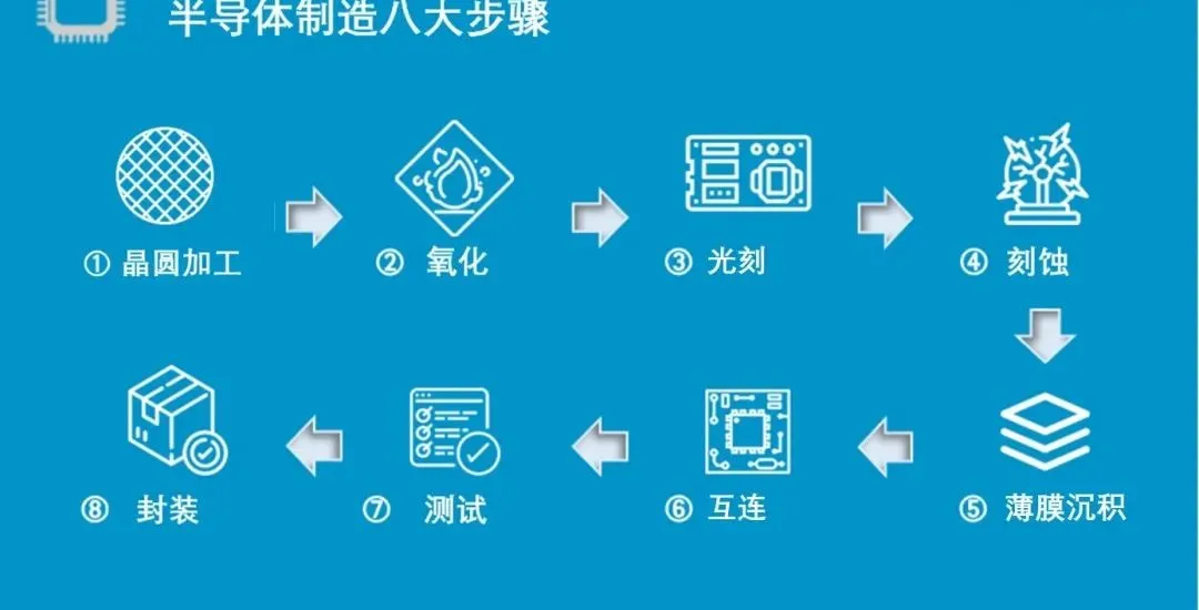
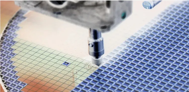
Every semiconductor product requires hundreds of processes. The Lam Group divides the entire manufacturing process into eight steps: wafer processing – oxidation – photolithography – etching – thin film deposition – interconnection – testing – packaging.
Step 1: Wafer Processing
① Ingot Casting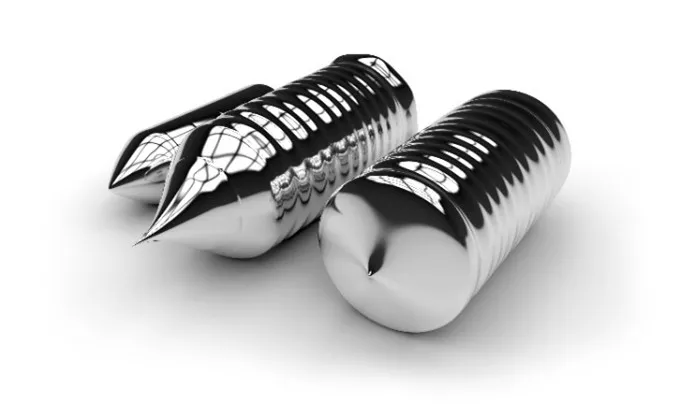
First, sand must be heated to separate carbon monoxide and silicon, and this process is repeated until ultra-pure electronic-grade silicon (EG-Si) is obtained. The high-purity silicon is melted into a liquid and then solidified into a single crystal solid form, known as an “ingot”. This is the first step in semiconductor manufacturing. The precision required for the production of silicon ingots (silicon rods) is very high, reaching the nanometer level, and the widely used manufacturing method is the Czochralski method.② Ingot CuttingAfter the previous step is completed, the ends of the ingot need to be cut off with a diamond saw, and then it is sliced into thin wafers of a certain thickness. The diameter of the ingot slices determines the size of the wafers; larger and thinner wafers can be divided into more usable units, helping to reduce production costs. After cutting the silicon ingot, “flat zones” or “notch” markings must be added to the slices to facilitate setting the processing direction in subsequent steps.③ Wafer Surface PolishingThe slices obtained from the cutting process are called “bare chips”, which are unprocessed “raw wafers”. The surface of the bare chips is uneven and cannot directly print circuit patterns on them. Therefore, it is necessary to first remove surface defects through grinding and chemical etching processes, then polish to form a smooth surface, and finally clean to remove residual contaminants, resulting in a clean finished wafer.
Step 2: Oxidation
The oxidation process serves to form a protective film on the wafer surface. It protects the wafer from chemical impurities, prevents leakage currents from entering the circuit, prevents diffusion during ion implantation, and prevents the wafer from slipping during etching.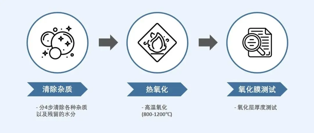 Dry Oxidation and Wet Oxidation
 In addition to oxidizing agents, other variables can affect the thickness of the silicon dioxide layer. First, the wafer structure, its surface defects, and internal doping concentration all influence the rate of oxide layer formation. Additionally, the higher the pressure and temperature generated by the oxidation equipment, the faster the oxide layer is formed. During the oxidation process, dummy wafers are also used based on the position of the wafer in the unit to protect the wafer and reduce the variation in oxidation.
Step 3: Photolithography
Photolithography is the process of “printing” circuit patterns onto the wafer using light. We can understand it as drawing the floor plan required for semiconductor manufacturing on the wafer surface. The finer the circuit pattern, the higher the integration of the finished chip, which must be achieved through advanced photolithography technology. Specifically, photolithography can be divided into three steps: coating photoresist, exposure, and development.① Coating PhotoresistThe first step in drawing circuits on the wafer is to coat the photoresist on the oxide layer. The photoresist changes the chemical properties to make the wafer act like “photo paper”. The thinner and more uniformly coated the photoresist layer on the wafer surface, the finer the patterns that can be printed. This step can be performed using the “spin coating” method.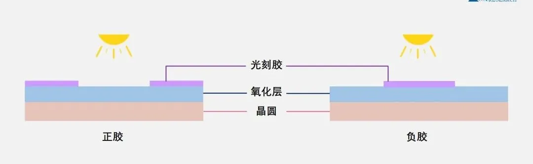 ② Exposure
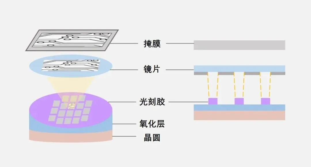 During the exposure process, the finer the printed pattern, the more components the final chip can accommodate, which helps improve production efficiency and reduce the cost of individual components. A currently notable new technology in this field is EUV lithography. Last February, the Lam Group, in collaboration with strategic partners ASML and imec, developed a brand new dry film photoresist technology. This technology significantly improves the productivity and yield of EUV lithography exposure processes by enhancing resolution (a key factor in fine-tuning circuit widths).③ Development
After exposure, the next step is to spray a developer on the wafer to remove the photoresist in the areas not covered by the pattern, revealing the printed circuit pattern. After development, various measuring devices and optical microscopes are used to check the quality of the drawn circuit.
The above is a brief introduction to wafer processing, oxidation, and photolithography processes. Next, we will introduce two important steps in semiconductor manufacturing: etching and thin film deposition!
Step 4: Etching
Etching methods are mainly divided into two types, depending on the substances used:Wet etching, which uses specific chemical solutions to remove the oxide film through chemical reactions, and dry etching, which uses gases or plasmas.Wet Etching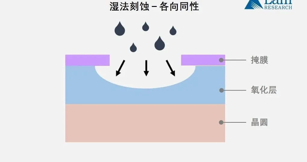 Dry EtchingDry etching can be divided into three different types. The first is chemical etching, which uses etching gases (mainly hydrogen fluoride). Like wet etching, this method is also isotropic, meaning it is not suitable for fine etching. The second method is physical sputtering, which uses ions in the plasma to strike and remove excess oxide layers. As an anisotropic etching method, sputter etching has different etching rates in horizontal and vertical directions, thus achieving higher precision than chemical etching. However, the downside of this method is that the etching speed is slower, as it relies entirely on physical reactions caused by ion collisions.
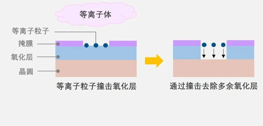 The last third method is Reactive Ion Etching (RIE). RIE combines the first two methods, using plasma for physical etching while also utilizing free radicals generated from plasma activation for chemical etching. In addition to achieving etching speeds that exceed the previous two methods, RIE can utilize the anisotropic characteristics of ions to achieve high-precision pattern etching.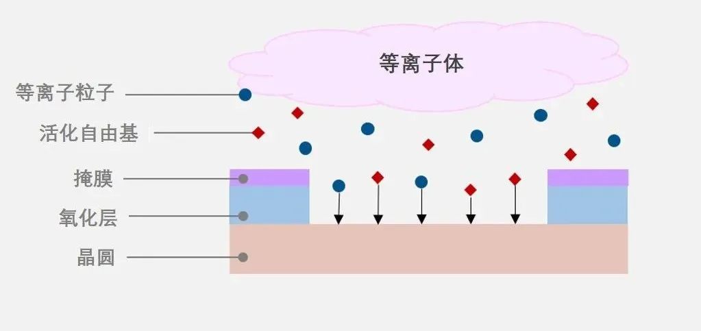
Step 5: Thin Film Deposition
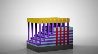 To form a multilayer semiconductor structure, we need to first create device stacks, which involves alternately stacking multiple layers of thin metal (conductive) films and dielectric (insulating) films on the wafer surface, followed by repeating the etching process to remove excess parts and form a three-dimensional structure. Techniques that can be used for the deposition process include Chemical Vapor Deposition (CVD), Atomic Layer Deposition (ALD), and Physical Vapor Deposition (PVD), with these methods further divided into dry and wet deposition.01.Chemical Vapor Deposition
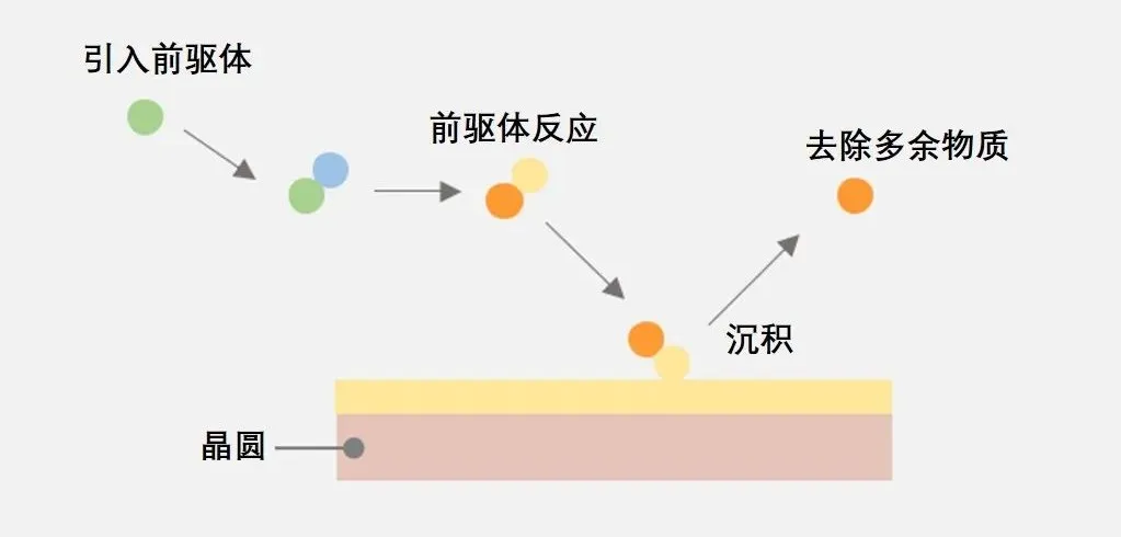 In Chemical Vapor Deposition, precursor gases undergo chemical reactions in the reaction chamber, generating thin films that adhere to the wafer surface and by-products that are extracted from the chamber. Plasma-Enhanced Chemical Vapor Deposition requires the use of plasma to generate reactive gases. This method lowers the reaction temperature, making it very suitable for temperature-sensitive structures. Using plasma can also reduce the number of deposition cycles, often resulting in higher quality films.02.Atomic Layer Deposition
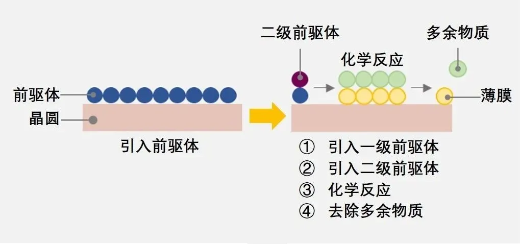 Atomic Layer Deposition forms films by depositing only a few atomic layers at a time. The key to this method is the independent steps that are performed in a specific order while maintaining good control. The first step is to coat the wafer surface with precursors, followed by introducing different gases to react with the precursors to form the desired material on the wafer surface.03.Physical Vapor Deposition
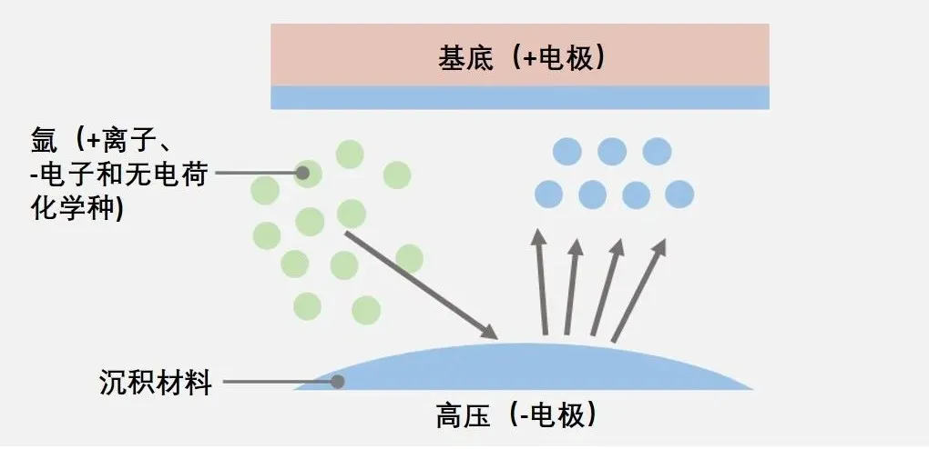 As the name suggests, Physical Vapor Deposition refers to the formation of films through physical means. Sputtering is a method of physical vapor deposition, where the principle is to use the bombardment of argon plasma to sputter atoms from the target material and deposit them on the wafer surface to form a film.In some cases, techniques such as Ultraviolet Thermal Processing (UVTP) can be used to treat the deposited films and improve their performance.The deposition equipment from the Lam Group boasts excellent precision, performance, and flexibility, including the ALTUS® series suitable for tungsten metallization processes, the SOLA® series with post-thin film deposition treatment capabilities, the SPEED® series for high-density plasma chemical vapor deposition, the Striker® series utilizing advanced ALD technology, and the VECTOR® PECVD series.
We have learned about the first few major steps in semiconductor manufacturing, including wafer processing, oxidation, photolithography, etching, and thin film deposition. We will continue to introduce the last three steps: interconnection, testing, and packaging, to complete the manufacturing of semiconductor chips.

Wuxi Qixin Semiconductor Technology Co., Ltd. is a high-tech enterprise specializing in the research, development, production, and sales of intelligent production equipment for the chip industry. Established in 2020, it is located in the Wuxi Huishan Economic and Technological Development Zone. The company has received multiple honors, including Wuxi Huishan District Pioneer Talent and Wuxi Taihu Talent, and is a council member of the Wuxi Semiconductor Association. The core members of the company’s R&D team all have over 20 years of experience in semiconductor equipment, with rich R&D experience in packaging processes and related equipment industrialization, holding multiple national-level technology invention, utility model patents, and software copyrights. The company has long-term industry-university-research cooperation with well-known domestic institutions such as Tsinghua University and the Chinese Academy of Sciences.
The self-developed MGP intelligent chip packaging system, AM fully automatic chip packaging system, and TF unit modular chip automatic cutting and forming system have all been recognized by the market and received unanimous praise from customers.
Wuxi Qixin Semiconductor Technology Co., Ltd. adheres to the values of innovation, efficiency, quality, and integrity, based in Wuxi, with the mission of creating intelligent equipment for China’s independent brand chips, supporting the chip industry, and building smart factories. It aims to become a leader in the chip packaging and testing equipment industry!
Disclaimer: This article is a network reprint or adaptation, and the copyright belongs to the original author. However, due to numerous reprints, it is impossible to confirm the true original author, hence the source is indicated. If there are any copyright issues, please contact us for deletion! The content of this article reflects the views of the original author and does not represent the views of this public account or its responsibility for authenticity.