Backside Power Delivery Technology (BSPDN)
Backside Power Delivery Technology requires separation of signals and power, placing the signal structure and power structure from wafer fabrication on the front and back of the wafer.
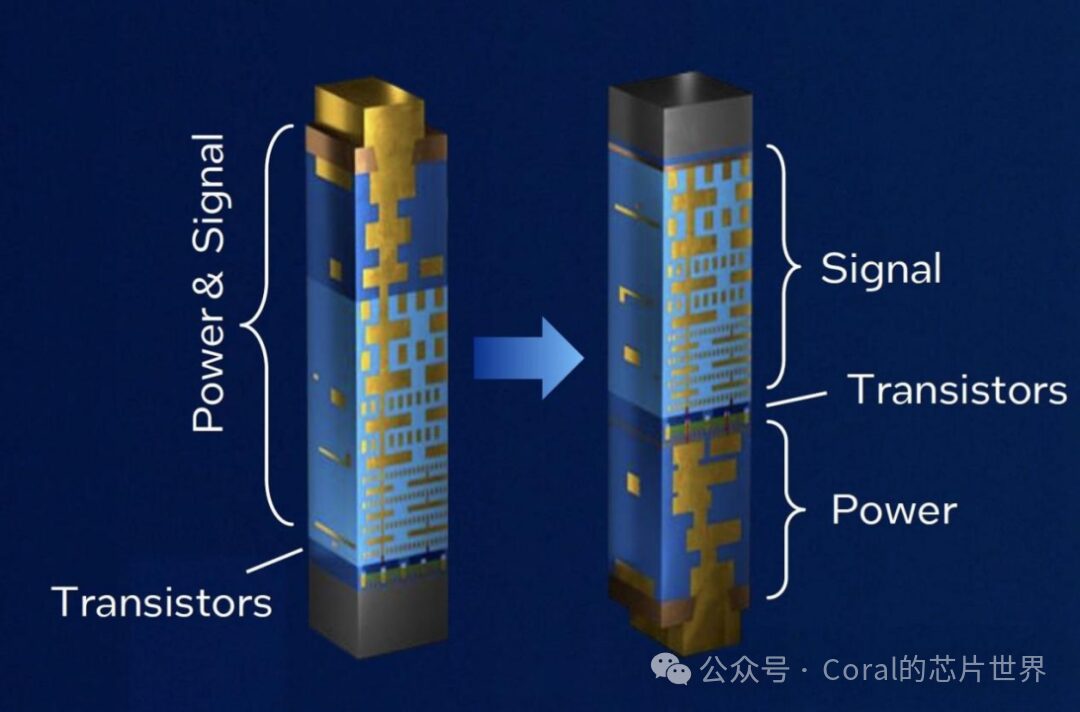
Illustration of Mainstream Chip Structure and Backside Power Chip Structure

Mainstream Chip Structure
Traditionally, the power and signal structures in chips are produced using back-end (metalization) processes (BEOL), completing circuit fabrication on the front side of the wafer. During the manufacturing process, the bottom key transistor layer is created first, and then continuous signal and power layers are built on top.
Frontside Power Structure
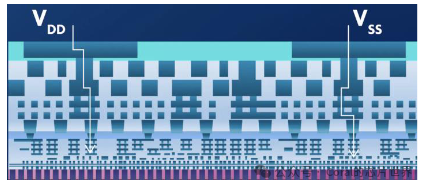
Both the signal structure and power structure are the electrical signal structures within transistors, the signal structure controls the operation or data of the transistor layer, and the power structure supplies power to the transistors.
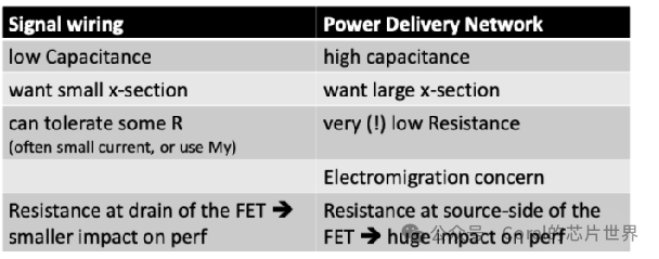
Signal Structure & Power Structure Design and Manufacturing Requirements
As integrated circuits become larger in scale and more complex in integration, to achieve better signal quality, power distribution, and chip heat dissipation, the dimensions of the signal and power structures are increasing.

Backside Power Chip Structure
Backside power moves the power structure to the back of the silicon wafer, separating the power structure and signal structure in the chip, which can reduce signal interference and facilitate management, optimizing the power structure, providing more possibilities in chip design and manufacturing.
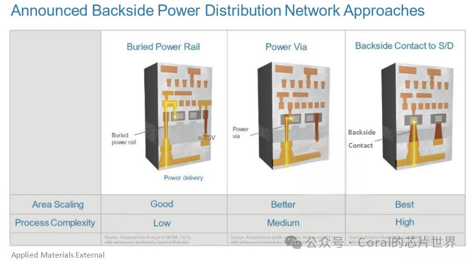
Classification of Backside Power Chip Structures
The contact top metal line structure in the Back Side Buried Power Rail (BSBPR/BPR) is buried within the silicon substrate beneath the transistors and in shallow trench isolation oxide, serving as the VDD and VSS power rails in the BEOL standard cell hierarchy.
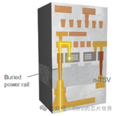
BSBPR/BPR Structure
Power Via is a metal line structure for wiring on the side of the transistor, Intel’s backside power chip solution creates a via that connects to one side of the transistor unit, without the power rail in the logic unit. Power is transmitted directly from the backside network to the unit or transistor contacts. This method is complex but enhances power efficiency and allows for scaling down the area of the transistor unit.
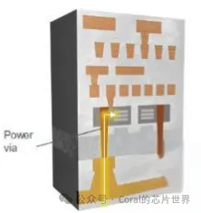
Power Via Structure
Backside Contact to Source & Drain is a metal line structure wired from the bottom, connecting power from the backside of the wafer to the source and drain of each transistor. The backside contact scheme can improve chip wiring, enhance electrical performance and has potential for increased chip-level density, but it has more stringent process requirements.
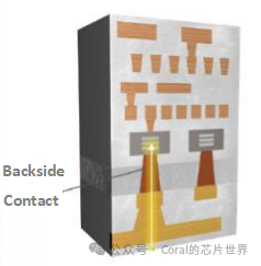
Backside Contact Structure


WeChat ID|Coral Semi
Official Account|Coral’s Chip World

·END·