In response to the challenges of declining yield and increasing costs for ultra-large-scale integrated circuits under advanced processes, chiplet technology divides large chips into multiple smaller chiplets, each manufactured independently, thus better controlling the manufacturing process, improving yield, and reducing costs. Moreover, different chiplets can adopt optimal process technologies, overcoming the limitations of a single process while effectively enhancing the reusability of intellectual property cores and shortening the R&D cycle.
Combining different types of chiplets into integrated chips and constructing optimal chiplet decomposition-combination design methods based on target applications is an important technical challenge. The decomposition of chiplets needs to consider the performance, cost, and safety of the integrated chip. The combination of chiplets is a complex optimization problem that filters out the optimal chiplets from the existing chiplet library based on application needs.
Additionally, the interconnection between chiplets is fundamental for data transmission and processing, significantly affecting data communication performance and power consumption. This includes core technologies such as interconnection topology, routing, fault tolerance mechanisms, interface protocols, and high-speed interface circuits. Within chiplet interconnection interfaces, there remain several scientific issues, such as new circuits that break through power consumption bottlenecks, reconfigurable transceivers compatible with different channels, adaptive detection and correction mechanisms, and automated cross-process migration of interface circuits. Addressing these challenges requires interdisciplinary research involving expertise in circuit design, electromagnetic signal integrity analysis, thermal management, and manufacturing processes.
Moreover, as the integration scale of chiplets increases, their power supply systems face new challenges; achieving power circuits capable of delivering hundreds or even thousands of watts within compact packages is a critical issue that needs to be addressed. With the increase in integration scale, the complexity of chiplet design also develops exponentially, necessitating improvements in automated design methods, including three-dimensional collaborative optimization design that incorporates advanced packaging and establishing multi-physics simulations and system-level verification.
In light of the many challenges and opportunities presented by the development of chiplet technology, the journal “Integrated Circuits and Embedded Systems” has specially planned the publication of the “Chiplet Research Column,” covering the latest advancements and innovative technologies in chiplet interface circuit design, coding techniques, noise elimination technologies, and more. This column aims to showcase the latest research progress and academic achievements in integrated circuit chiplet technology, promote academic exchanges in the chiplet field, drive the development and breakthroughs of key technologies, and provide theoretical and technical support for the advancement of chiplet technology in China. This research column is published in the 2nd issue of 2024.
The following six articles are included (click to read the full text or download the complete PDF version):
Chiplet Technology: Expanding New Boundaries in Chip Design
Development and Challenges of Chiplet Technology
Chord and Signaling Techniques for Noise Elimination in Chiplet Interconnect Data Interfaces
Review of Heterogeneous Integrated Interconnection Interfaces
Chiplet Function Partitioning Methods and Interconnection System Review
Substrate Integrated Waveguide Ultra-Wide Stopband Filter Power Divider Based on Lateral Coupling and Orthogonal Coupling
Li Jiayao, Zhang Kun, Pan Quan
(Southern University of Science and Technology, Shenzhen 518055)
Abstract: Chiplet technology is a method that integrates multiple small chips into a complete system chip, aiming to achieve chip reuse, heterogeneous integration, performance enhancement, and cost reduction. The focus of this technology’s development mainly includes heterogeneous integration, new interconnections, and new packaging. Among these, interface interconnection is key to chiplet technology. Interface interconnection includes physical layer interfaces and data transmission protocols, and the design of interfaces and protocols must consider factors such as process technology, packaging technology, power consumption limitations, and requirements of upper-layer applications. Serial interconnection and parallel interconnection are two options for chip-to-chip physical layer interfaces. Furthermore, new interconnection technologies like optical interconnections and wireless interconnections have emerged for different transmission media, providing higher bandwidth, lower power consumption, and more flexible interconnection topologies. In the future, chiplet technology is expected to bring significant breakthroughs and developments to the electronics field, promoting more efficient, flexible, and innovative chip design and manufacturing.

Reference format: Li Jiayao, Zhang Kun, Pan Quan. Chiplet Technology: Expanding New Boundaries in Chip Design [J]. Integrated Circuits and Embedded Systems, 2024, 24(2): 1-9.
Liu Chaoyang, Ren Bolin, Wang Zedong, Lv Fangxu, Zheng Xuqiang
(1. Institute of Microelectronics, Chinese Academy of Sciences, Beijing 100029; 2. College of Computer Science, National University of Defense Technology, Changsha 410073)
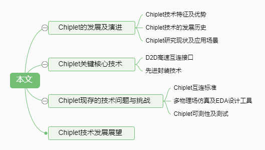
Abstract: As semiconductor process dimensions gradually approach physical limits, the improvements in chip power consumption, performance, and area brought by process advancements become increasingly marginal, marking the entry of semiconductor technology into the “post-Moore era.” To further meet the high bandwidth communication demands arising from the rapid development of information communication industries such as machine learning and artificial intelligence, chiplet technology based on advanced interconnection and packaging technologies has come into our view. Chiplet technology breaks down the original complex multifunctional SoC chips into multiple small-area, low-cost chips of different process nodes, which are then reassembled. Due to its high yield, low cost, high integration, powerful performance, good flexibility, and fast time-to-market, it has garnered significant attention from both academia and industry. This paper reviews and elaborates on the technical characteristics, advantages, development history, and specific applications of chiplet technology, while detailing the key core technologies of chiplets, especially chiplet D2D interconnection technology. Finally, it discusses the existing technical issues and challenges facing chiplet technology and provides future development suggestions.
Reference format: Liu Chaoyang, Ren Bolin, Wang Zedong, et al. Development and Challenges of Chiplet Technology [J]. Integrated Circuits and Embedded Systems, 2024, 24(2): 10-22.
Han Chenxi, Zhao Xiaoteng, Liu Yuan, Zhang Qi, Liu Shubin, Zhu Zhangming
(Xi’an University of Electronic Science and Technology, Xi’an 710071)
Abstract: Chiplet technology can improve the yield of integrated chips, reduce R&D costs, and enhance efficiency, making it a current research hotspot. High-speed data interfaces are required for interconnect communication between different chiplets. To enhance overall bandwidth density, chiplet interconnections often use single-ended signal transmission, which can be affected by common-mode noise, synchronous switch noise, and crosstalk noise. Chord and signaling techniques convert single-ended signals into pseudo-differential signals through encoding and decoding of transmitted data, which can suppress noise and improve signal transmission quality. Additionally, as a modulation method, chord and signaling techniques are independent of process and architecture, offering good process portability, thus gaining widespread application. This paper reviews common chord and signaling techniques, analyzes and summarizes their performance parameters, and finally discusses the future development of chord and signaling techniques.

Reference format: Han Chenxi, Zhao Xiaoteng, Liu Yuan, et al. Chord and Signaling Techniques for Noise Elimination in Chiplet Interconnect Data Interfaces [J]. Integrated Circuits and Embedded Systems, 2024, 24(2): 23-30.
Li Peijie, Liu Qinrang, Chen Ting, Shen Jianliang, Lv Ping, Guo Wei
(Information Engineering University of the Strategic Support Force of the People’s Liberation Army, Zhengzhou 450002)
Abstract: With the development of integrated circuits towards the post-Moore era, heterogeneous integration technology has become an emerging direction in microelectronics. Heterogeneous integrated interconnection interfaces are key to heterogeneous integration technology and are crucial for heterogeneous integrated chips and systems. To further promote the realization of heterogeneous integrated interconnection interfaces, this paper analyzes the structures of existing heterogeneous integrated chips and systems, summarizing heterogeneous integration technology into four technical routes: small chiplet splicing into large chips, large chips splicing into large chips, wafer-level chips, and wafer-level systems. It compares and summarizes the characteristics of heterogeneous integrated interconnection interfaces under different technical routes, elaborating on the current research status and existing issues in both industry and academia regarding heterogeneous integrated interconnection interfaces. Finally, it presents future development trends and necessary technical characteristics for heterogeneous integrated interconnection interfaces.

Reference format: Li Peijie, Liu Qinrang, Chen Ting, et al. Review of Heterogeneous Integrated Interconnection Interfaces [J]. Integrated Circuits and Embedded Systems, 2024, 24(2): 31-40.
Chen Long, Huang Letian
(University of Electronic Science and Technology of China, School of Integrated Circuit Science and Engineering, Chengdu 611731)
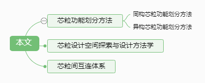
Abstract: Currently, chip design faces the challenge of the “area wall,” which brings high tape-out costs for chip manufacturing. Chiplet technology can manufacture smaller area chips using mature process technologies and then break the area wall limitation through advanced packaging methods, achieving agile chip design and reducing design costs. A core issue in utilizing chiplet technology is determining the optimal granularity of chiplet partitioning to meet the flexible needs of chip design. The function partitioning of chiplets also affects the interconnection structure between chiplets; how to achieve interconnections between functional chiplets is key to realizing the overall functionality of the chip. Therefore, this paper reviews recent research on chiplet function partitioning both domestically and internationally, explores the design space of chiplets, and discusses the impact of function partitioning on chiplet interconnection networks, pointing out that the methodology of chiplet design is an important research direction for the future development of chiplet technology.
Reference format: Chen Long, Huang Letian. Chiplet Function Partitioning Methods and Interconnection System Review [J]. Integrated Circuits and Embedded Systems, 2024, 24(2): 41-49.
Fan Chenhui, Liu Xiaoxian, Liu Nuo, Zhu Zhangming
(Xi’an University of Electronic Science and Technology, Xi’an 710071)
Abstract: The application of substrate integrated waveguide filter power dividers in communication systems is gradually expanding. Similar to traditional waveguide resonators, substrate integrated waveguide resonators contain multiple transmission modes, making it challenging to achieve ultra-wide stopband characteristics in substrate integrated waveguide filters. This paper designs an ultra-wide stopband substrate integrated waveguide filter power divider realized by electrical excitation. Specifically, a fourth-order substrate integrated waveguide filter power divider based on electromagnetic alternating coupling topology is proposed, featuring electrical input and output ports. Lateral coupling is achieved through window openings on the side of the resonant cavity, while vertical coupling is realized by etching S-slot lines in the coupling window between adjacent cavities. The orthogonal transmission path can suppress multiple higher-order modes, and simulation and measurement results indicate that the stopband bandwidth exceeds 9f0 and 3.1f0, with the out-of-band suppression effect of the filter power divider at a center frequency of 35.5 GHz better than -20 dB. This method has been validated with physical experiments, and the test results are consistent with the simulation results.

Reference format: Fan Chenhui, Liu Xiaoxian, Liu Nuo, et al. Substrate Integrated Waveguide Ultra-Wide Stopband Filter Power Divider Based on Lateral Coupling and Orthogonal Coupling [J]. Integrated Circuits and Embedded Systems, 2024, 24(2): 50-56.

Column Editor:
Liu Shubin

Welcome to submit articles to our journal’s official website (www.jices.cn)