Imagine you have 32 beautiful women to manage; handling all 32 at once can be a bit tricky, right? No worries, let’s take it “slowly” one by one. Why do I put “slowly” in quotes? Because dealing with one is actually much faster than handling all 32 at once. Okay, let’s pause this beautiful fantasy and get to know the “territory” of bit banding.
The concept of bit banding: For the 51 microcontroller, there are only 8 bits, while for the M3, there are 32 bits. This means that one specific bit among the 32 can be manipulated using a simple address transformation algorithm. It can be mapped to an address space, meaning that one bit occupies one address. It’s like placing Huizhou at a specific address in Guangdong Province, named Huizhou City. You can get to Huizhou City by taking a ticket to Huizhou, but don’t go to Dongguan! However, this bit is only valid at the lowest address, because the address may point to a 32-bit memory unit, and because it is LSB (Least Significant Bit) valid, you don’t need to mask other bits when manipulating the bound bit. Since only the lowest bit is valid, you only need to check the lowest bit, because you bought a ticket to Huizhou, so there’s no need to mask Dongguan; the bus won’t go to Dongguan. Please see the “beautiful” photo:
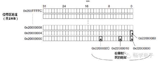
From the image, we can see that one bit is bound to one address. Do you find it strange? Why does the bit-banding area start at 0x2000 00000 while the bound address starts at 0x2200 0000? Ah, don’t rush; as they say, haste makes waste.
Since the M3 core processes everything in 32-bit chunks and does not operate on individual bits separately, bit banding allows the CPU to manipulate an individual bit with just one instruction cycle, and the speed is evident. However, the entire M3 core does not allow bit banding everywhere; it only has two areas that do:
SARM area: 0x2000_0000 to 0x200F_FFFF, and the bound address for this SRAM starts at 0x2200 0000.
On-chip peripheral area: 0x4000_0000 to 0x400F_FFFF, and the bound address for this area starts at 0x4200 0000.
The mapping tables are as follows:
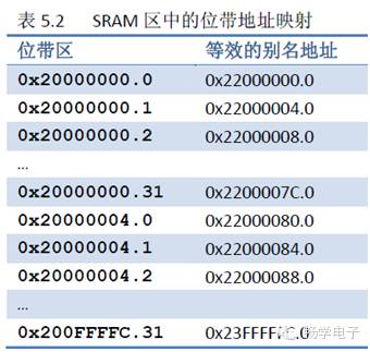
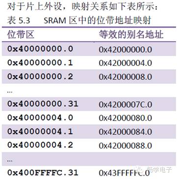
Now you know why, right? If you still don’t know, come here and let me tease you for 10 minutes.
If you know, come here and let me treat you to ten more beauties.
So how do we bind? What about the algorithm mentioned at the beginning? Actually, calling it an algorithm might sound intimidating, as many think algorithms are complex. In reality, it just involves two formulas (one for SRAM, one for on-chip peripherals) as follows, where A is the byte’s address, and n is the bit sequence number:
SRAM area mapped address AliasADDr = 0x22000000 + ((A – 0x20000000) * 8 + n) * 4 = 0x22000000 + ((A – 0x20000000) * 32 + n * 4
On-chip peripheral area mapped address AliasADDr = 0x42000000 + ((A – 0x20000000) * 8 + n) * 4 = 0x42000000 + ((A – 0x20000000) * 32 + n * 4
Okay, with this algorithm, we can start programming in C.
First, let’s find the addresses of GPIOA~E; hover the mouse over GPIOA~E, right-click,
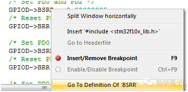
You can see the GO TO Definition; click it to find the addresses of GPIOA~E, and similarly, we can find the “big boss” behind them, as shown in the figure:
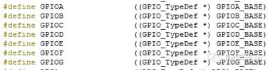
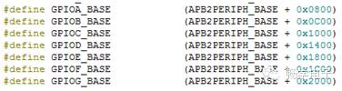


Alright, we have the addresses, but we also need the offset addresses for the input/output registers of each IO port:


That’s right, let’s take 0x08 and 0x0C as examples:
1 #define GPIOA_ODR_A (GPIOA_BASE + 0X0C)
2 #define GPIOA_IDR_A (GPIOA_BASE + 0X08)
3 …
4 #define GPIOA_ODR_E (GPIOE_BASE + 0X0C)
5 #define GPIOA_IDR_E (GPIOE_BASE + 0X08)
6
7 #define BitBand(Addr,BitNum) *((volatile unsigned long *)(Addr&0xf0000000)+0x2000000+((Addr&0xfffff)<<5)+(BitNum<<2))
8
9 #define PAout(n) BitBand(GPIOA_ODR_A,n)
10 #define PAin(n) BitBand(GPIOA_IDR_A,n)
11 …
12 #define PEout(n) BitBand(GPIOE_ODR_A,n)
13 #define PEin(n) BitBand(GPIOE_IDR_A,n)
Let me explain:
Addr&0xf0000000 is used because we don’t know whether it’s in the SRAM or on-chip peripheral area, so we take the highest bit, which could be 4 or 2.
Addr&0xfffff shows the range of bit banding: 0x2000_0000 to 0x200F_FFFF and 0x4000_0000 to 0x400F_FFFF, so we mask the top three bits, which is equivalent to A – 0x20000000.
Why do I use <<5 and <<2 here? If you compare, you can see that <<5 is equivalent to *32 and <<2 is equivalent to *4. Why do we use left shift instead of multiplication? The reason is that left shifting is much faster than multiplication, so we try to convert multiplication and division into addition, subtraction, and left/right shifts.
Writing this, it’s correct. Now we can easily manipulate a 32-bit chip like we did with the 51…
I am not talented; if I made any mistakes, please feel free to point them out as if you were catching corruption. I humbly seek your guidance and hope you can understand…