Recently, I had a conversation with Academician Lu Zhiyuan from the Chinese Academy of Sciences about semiconductors. This veteran expert has been involved in chip development for decades, and listening to him is truly more enlightening than reading ten years’ worth of books.
When it comes to nanometer-level chip manufacturing, Academician Lu directly told me: “The lithography machine is the biggest bottleneck.” This statement was particularly straightforward, without any roundabout pleasantries.
01 How Difficult is Nanometer-Level Manufacturing?
Academician Lu gave me an analogy: “Imagine engraving a map of the entire city of Beijing on the cross-section of a single hair strand.” This illustrates the precision requirements for a 3-nanometer chip.
To be honest, this analogy shocked me. The diameter of a hair is about 80 micrometers, while 3 nanometers is only one-thirtieth-thousandth of a hair’s width! At such a small scale, traditional processing methods are completely inadequate.
Moreover, at the nanometer level, quantum effects begin to take effect, and electrons no longer behave predictably. They tend to scatter everywhere, posing a significant challenge for chip design.
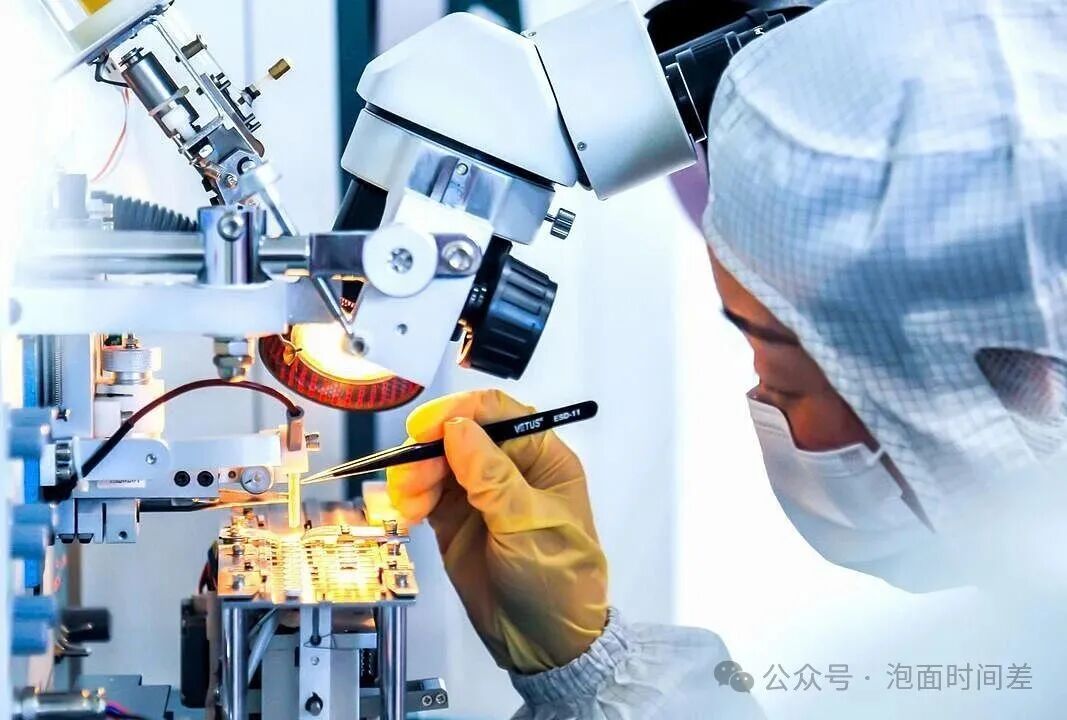
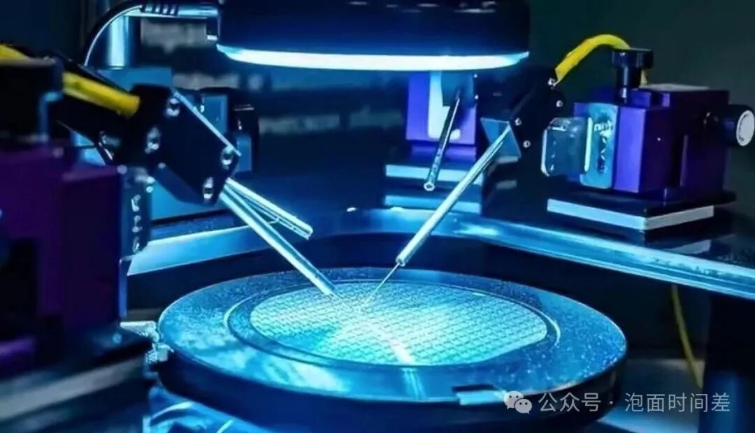
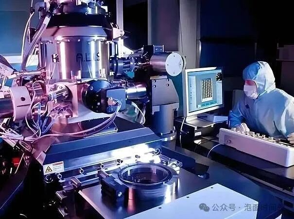
02 Lithography Machines: The Key Bottleneck
When discussing lithography machines, Academician Lu’s tone became noticeably serious: “It’s like a surgeon’s scalpel; without a good knife, even the most skilled doctor cannot perform well.”
Currently, the most advanced EUV lithography machines can only be produced by ASML in the Netherlands. Each machine costs over $200 million, and there is a queue to purchase one; they may not even sell it to you.
Academician Lu informed me that the core technology of lithography machines involves precision optics, ultra-precision mechanics, vacuum technology, materials science, and several other fields. “This is not just a simple accumulation of technologies, but a systematic engineering breakthrough,” he described.
The most troublesome aspect is that EUV lithography uses extreme ultraviolet light with a wavelength of 13.5 nanometers, which cannot propagate in air. The entire system must operate in a vacuum environment, making the technical challenges evident.
03 China’s Path to Breakthroughs
However, Academician Lu is not pessimistic. He told me: “Chinese people have never been afraid of difficulties; the key is to find the right path.”
Shanghai Microelectronics has made breakthroughs in 28-nanometer lithography machines. Although there is still a gap compared to the most advanced 3-nanometer technology, it can already meet many application needs.
More importantly, we are also laying out new lithography technologies, such as electron beam lithography and multi-beam lithography, which may allow us to overtake competitors.
Academician Lu specifically mentioned that the Institute of Optoelectronic Technology at the Chinese Academy of Sciences has already reached a world-leading level in lithography lens technology. “Lithography machines are a system engineering project; we need to break through one component at a time.”
04 Where is the Hope for the Future?
At the end of our conversation, I asked Academician Lu what his views on the future were, and his answer left a deep impression on me.
“Moore’s Law is nearing its end, which ironically presents an opportunity for China,” he explained. When traditional scaling routes encounter physical limits, everyone must find alternative paths.
For example, 3D stacking technology, new material applications, quantum computing, etc. In these new arenas, China is not far behind compared to foreign countries, and in certain fields, we even have advantages.
Especially in application-oriented areas like AI chips and IoT chips, China’s vast market serves as the best testing ground. “The development of technology ultimately needs to return to applications,” Academician Lu summarized.
After talking with Academician Lu, my biggest takeaway is that in technology, one cannot be overly impatient, but neither should one underestimate oneself. China’s semiconductor industry is steadily advancing; although the road ahead is long, the direction is correct.
Honestly, listening to this veteran expert discuss technology is far more insightful than reading those analytical articles online. His decades of expertise can pinpoint the crux of the matter in just a few words.
That’s all for today’s sharing. If anyone has further questions about semiconductor technology, feel free to leave comments for discussion!