Click the card below to follow Arm Technology Academy
This article is authorized to be reprinted from the WeChat public account Electronic Circuit Development Learning. This article mainly shares how to build a Cortex-M3 soft core on FPGA.
Abstract: This article describes how to build a Cortex-M3 soft core processor on FPGA based on Xilinx Artix-7™ series FPGA. It introduces how to customize an Arm Cortex-M3 SoC soft core, add GPIO and UART peripherals, develop applications using the Keil MDK environment, and download and debug Arm programs using Jlink. The final implementation effect is LED blinking and serial output of Hello World information.

Figure 1
1 Necessary Basic Knowledge
To complete the implementation of the Arm Cortex-M3 soft core on FPGA faster, some necessary basic knowledge is essential!
Basic knowledge of FPGA development, such as FPGA development process, design, synthesis, layout, routing, constraints, and downloading. Basic usage of Xilinx Vivado development environment, such as Block Design design method, pin allocation, Bitstream file generation and downloading. Basic usage of Arm Cortex-M3 core, such as development of STM32, MM32, GD32, CH32 microcontrollers. Basic usage of Keil-MDK development environment, basic project creation, compilation, and downloading process. If you have all the above knowledge, congratulations! You can complete the implementation of the Arm Cortex-M3 soft core on FPGA within 2 hours.
2 Download Cortex-M3 FPGA IP Core
First, we need to obtain the Arm Cortex-M3 FPGA soft core IP package from the Arm official website.
The download link is as follows:
https://silver.arm.com/browse/AT426File name: Cortex-M3 DesignStart FPGA-Xilinx edition (r0p1-00rel0)
File size: 7.52MB
MD5SUM: cd67536c29023429cde47130d51b6f49
You need to register an account on the official website to download. After obtaining the download link, copy it to the browser to download.
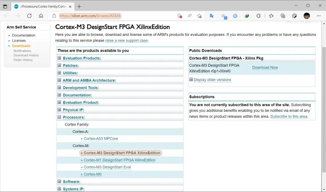
Figure 2 Arm Official Website
After unzipping the compressed package, there are a total of 4 folders:
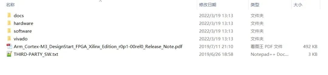
Figure 3 Contents of the Compressed Package
The contents of each folder are as follows:
●docs: Stores the Arm Cortex-M3 processor reference manual, DesignStart FPGA version usage instructions, top-level Block Design block diagram based on Arty-A7 development board, and other files.
●hardware: Stores the Vivado project based on Digilent Arty-A7 development board, top-level Block Design file, pin constraint file, Testbench file, etc.
●software: Stores the Keil-MDK project, SPI Flash programming algorithm file, etc.
●vivado: Contains the IP core files of the DesignStart Cortex-M3 Xilinx FPGA version, where the Arm_ipi_repository folder contains the core source files. The contents of the IP files are encrypted and not readable.
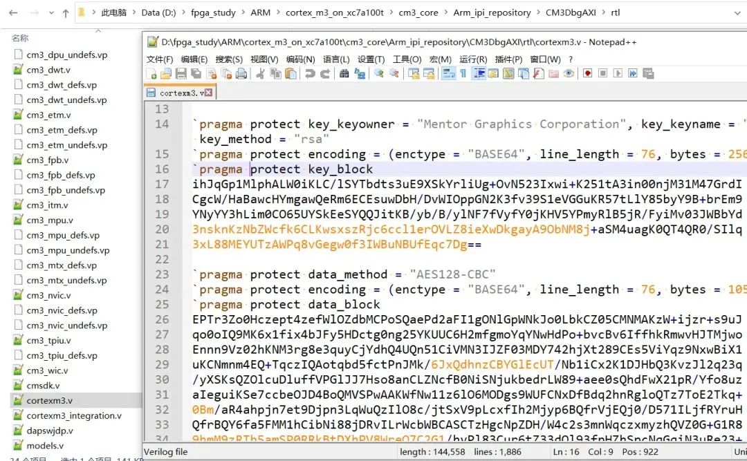
Figure 4 IP Core Source Code
3 Hardware Preparation
To complete the DS CM3 on FPGA, we need at least the following hardware:
● An Artix-7™ development board to build the Cortex-M3 soft core SoC. I am using the ZYBO development board, with FPGA model XC7A100T.
● A Xilinx FPGA downloader to download the soft core Bitstream to the FPGA, such as Platform USB Cable, JTAG-HS2/HS3, etc.
● An Arm Cortex-M3 debugger to debug the Arm core program download and debugging, such as JlinkV9, Jlink-OB, etc.
The official DS CM3 IP core is based on Digilent’s Arty-A7 development board, with FPGA model XC7A35T/100T, and Vivado version v2019.1. If you happen to have this development board, you can directly use the official example project.
Digilent Arty-A7 Development Board:
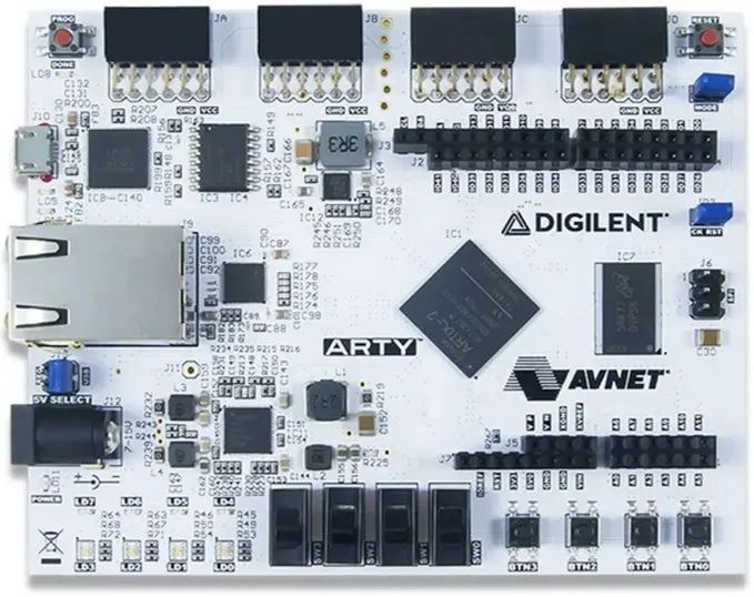
Figure 5 Arty-A7 Development Board
ZYBO Development Board:
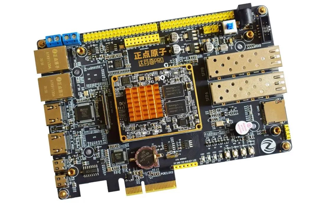
Figure 6 ZYBO Development Board
4 Software Preparation
● Xilinx Vivado development environment, the official recommended version is above 2018.2, I am using version 2018.3
● Keil MDK development environment, such as version 5.33
● DS_CM3’s Keil device package
Download the device support package specifically for DesignStart Cortex-M3 from the Keil official website. The download link is as follows:
https://keilpack.azureedge.net/pack/Keil.V2M-MPS2_DSx_BSP.1.1.0.pack5 Building the Cortex-M3 Soft Core
Once the above software and hardware are ready, we can start building the Cortex-M3 soft core.
First, create a folder named cortex_m3_on_xc7a100t to store all project files for this example, and create the following folders:
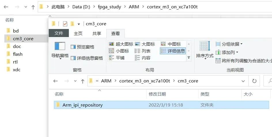
Figure 7 Directory Structure
The function of each folder:
● bd folder: Used to store Block Design designs
● cm3_core folder: Used to store Arm Cortex-M3 core IP core files
● doc folder: Used to store design documents
● flash folder: Used to store generated bit and mcs files
● rtl folder: Used to store user-designed Verilog source files
● xdc folder: Used to store pin and timing constraint files
Among them, the cm3_core folder needs to copy the Arm_ipi_repository folder from the official compressed file, with the path being AT426-BU-98000-r0p1-00rel0
evado”>Arm_ipi_repository
After preparing the above folders, we can start creating the project.
5.1 Create Vivado Project
Open Vivado 2018.3, open the project creation wizard, enter the project name, and the project storage path is the folder we just created.
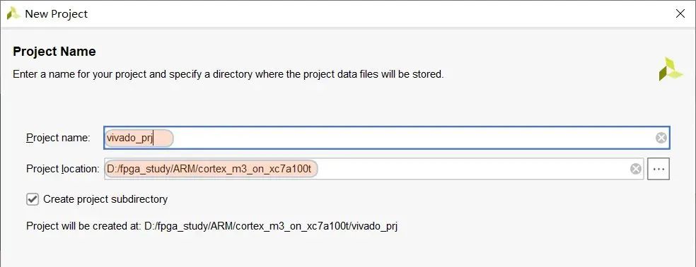
Figure 8 Create Project
Select the complete model of the FPGA chip: XC7A100TFGG484.
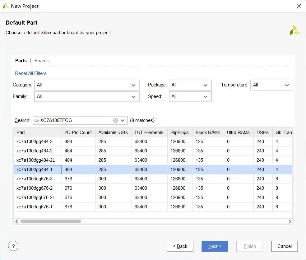
Figure 9 Select Chip Model
The project directory after completion of creation.
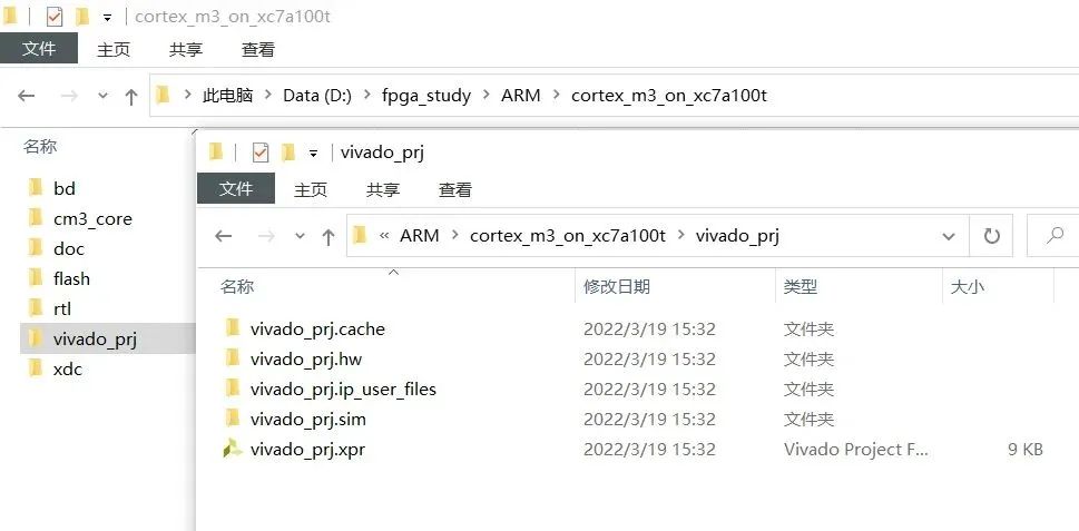
Figure 10 Vivado Project Directory
5.2 Add IP Core Search Path
To search for the Arm Cortex-M3 processor IP core in Block Design, we need to add the path where the Arm soft core IP is located to the search path.
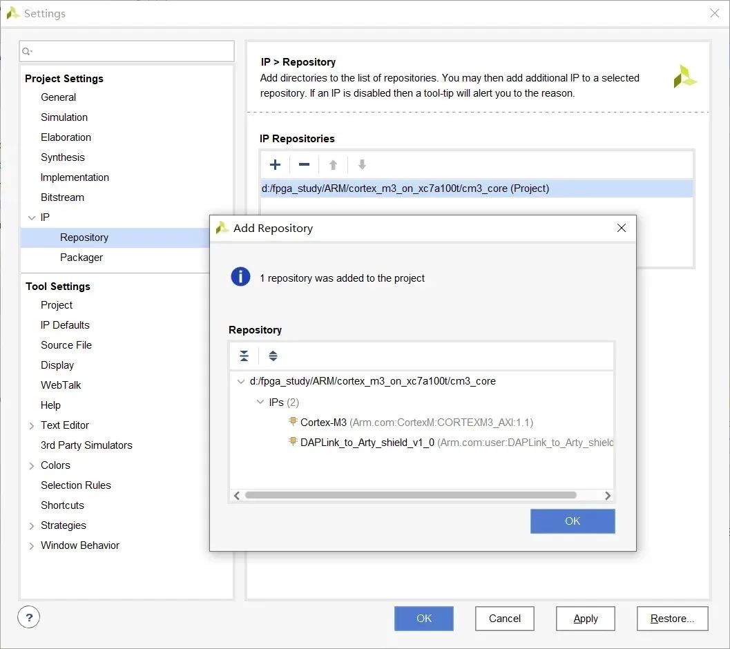
Figure 11 Add to Search Path
5.3 Create Block Design
To facilitate the graphical connection of each IP core in the future, we use the Block Design graphical design method, which allows us to quickly build a customized soft core processor.
Create a new Block Design, name it cm3_core, and save it in the bd folder created earlier.
Add the Cortex-M3 processor core to the canvas:
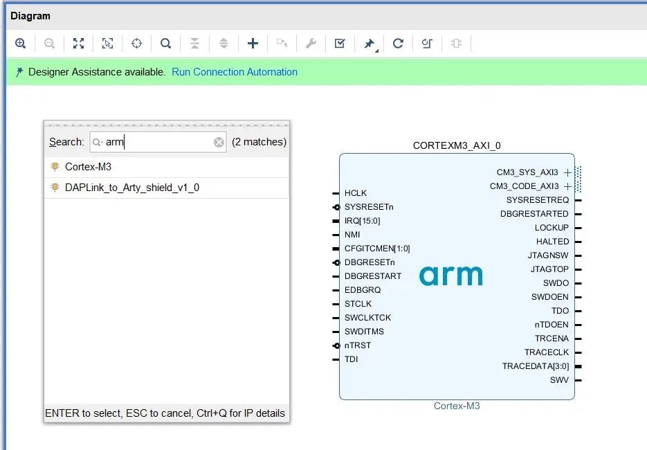
Figure 12 Add Arm Core
Double-click the Cortex-M3 IP core for some basic configuration. We do not need the Trace function, select No Trace, use SWD interface for debugging, and disable the JTAG port:
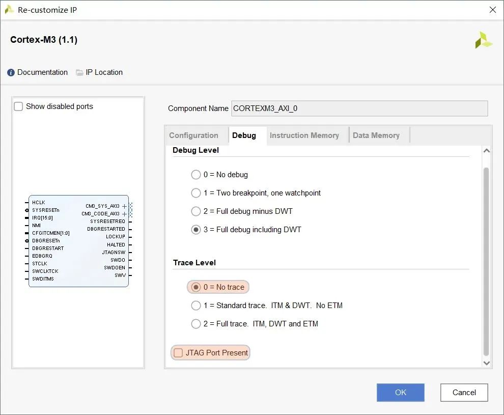
Figure 13 Configure Arm Core
Set the instruction space and data space size to 64KB, without initialization.
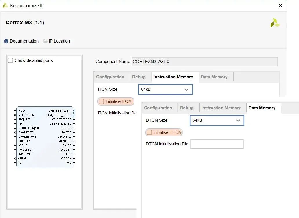
Figure 14 ITCM Core DTCM Configuration
5.4 Add Some Necessary IP Cores
● Clock PLL: Used to provide the core, bus, and peripheral clocks. Here we configure it to 50MHz single-ended input, and PLL output is also configured to 50MHz. If the clock frequency is set higher, synthesis will prompt that WNS and TNS timing do not meet, which may affect the normal operation of the system.
● Processor Reset IP: Used to provide the reset signal required by the core, peripherals, and interconnect components. No customization is needed, keep the default settings.
● Bus Interconnect IP: The Cortex-M3 core is AHB bus, and it has been internally converted to AXI3 bus. The GPIO/UART peripheral IP cores provided by Xilinx are AXI4-Lite bus, so we need to add a bus interconnect matrix to convert different protocols, with the number of slaves set to 1 and the number of masters set to 2, connected to the processor’s SYS bus.
● Basic Logic Gate IP: The Cortex-M3 core requires a low-level reset, while the reset IP outputs a high-level reset, so we need to insert a NOT gate in between for conversion.
* Constant IP: This soft core building does not involve the interrupt part, so IRQ and NMI are given constant 0. If interrupts need to be connected to the processor, multiple interrupt sources can be merged into one using the Concat core.
Add the above IP cores to the Block Design canvas and connect them as shown in the figure below:
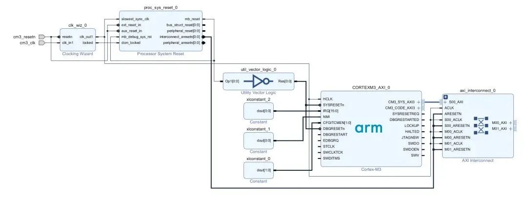
Figure 15 Schematic Connection
According to the official manual, the soft core IP provided by Arm includes ITCM and DTCM memory, so we do not need to add external BRAM as the storage area for programs and data.
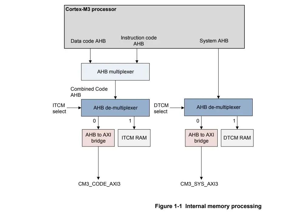
Figure 16 Cortex-M3 Core Structure
Both ITCM and DTCM provided in the core are based on RAM implementation, which means that when we use Keil to download the program, it is only downloaded to RAM, and data will be lost when power is off.
Thus, the Arm Cortex-M3 processor core has been built, and we will now add GPIO and UART peripherals.
5.5 Add GPIO and UART Peripherals
Some commonly used microcontrollers, such as STM32, generally have a fixed number of peripherals like TIM, UART, SPI, CAN, etc., while using FPGA to build the Arm soft core SoC is more flexible. If you do not need SPI, you do not need to add SPI peripherals. If you need 10 UARTs, just add 10 UARTs. The configuration of peripherals is quite flexible, but of course, these peripherals are implemented based on FPGA logic resources, and the actual number added will be limited by the size of the FPGA chip’s logic resources.
Below, we will take adding a set of AXI GPIO and a set of AXI UART as an example to illustrate how to use the Arm soft core to control these two peripherals.
The AXI GPIO peripheral provided by Xilinx has the following characteristics:
● There are two channels internally, Channel 1 and Channel 2, each channel supports up to 32 pins
● Each pin can be configured as input or output mode
● Each pin can set a reset initial value
● Supports interrupt output
The provided AXI UART peripheral has the following characteristics:
● Full duplex
● Supports 5-8 data bits
● Supports parity check
● Configurable baud rate from 110 to 230400
Here we configure the GPIO as dual-channel, where channel 1 is output mode, and the lower 4 bits are used to connect to LED, while channel 2 is input mode, and the lower 4 bits are used to connect to buttons.
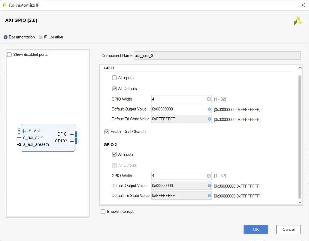
Figure 17 GPIO Configuration
UART is configured to a baud rate of 115200, 8 data bits, no parity check.
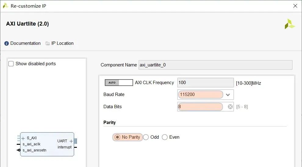
Figure 18 UART Configuration
After configuration, connect them to the master interface of the interconnect IP:
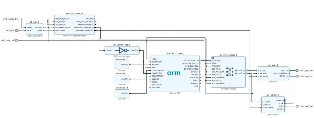
Figure 19 Schematic Connection
The clocks for these two IPs can use the same clock as the processor, and the reset can use the peripheral reset signal output from the reset IP.
5.6 SWD Interface Connection
In the official DesignStart IP core documentation, in addition to the Cortex-M3 processor, there is a DAP-Link debugging core. If you use a DAP-Link debugger, you need to add this IP core.
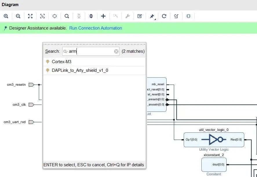
Figure 20 DAP-Link
Here we will not use the DAP-Link debugger, but rather use Jlink in SWD mode. The SWD mode requires two lines, one for SWCLK clock signal and one for SWDIO bi-directional data signal. The processor provides 3 pins: SWDI, SWDO, and SWDOEN. We also need to implement a bi-directional port module.
The bi-directional port module implemented based on IOBUF primitive is as follows:
module swdio_tri_buffer( //Inputs input swd_o, input swd_oe, //Outputs output swd_i, //Inouts inout swd_io);IOBUF swd_iobuf_inst( .O(swd_i), .I(swd_o), .IO(swd_io), .T(!swd_oe));endmoduleAdd it to our design.
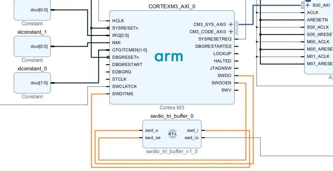
Figure 21 SWD Interface Connection
The final Block Design is shown in the figure below:
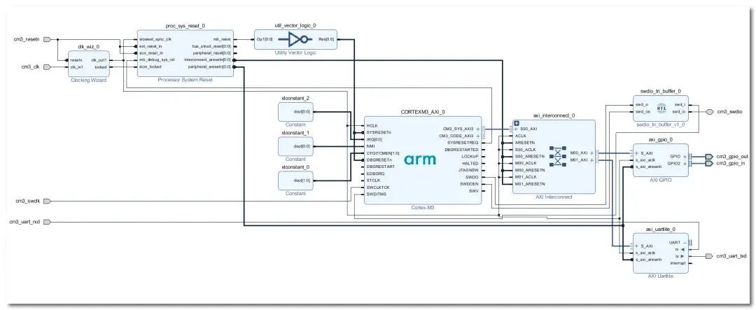
Figure 22 Schematic Connection
5.7 Allocate Peripheral Base Address
After adding the peripheral IPs, we also need to allocate base addresses and space for the peripherals. In the address editing box, right-click to select auto-allocate.
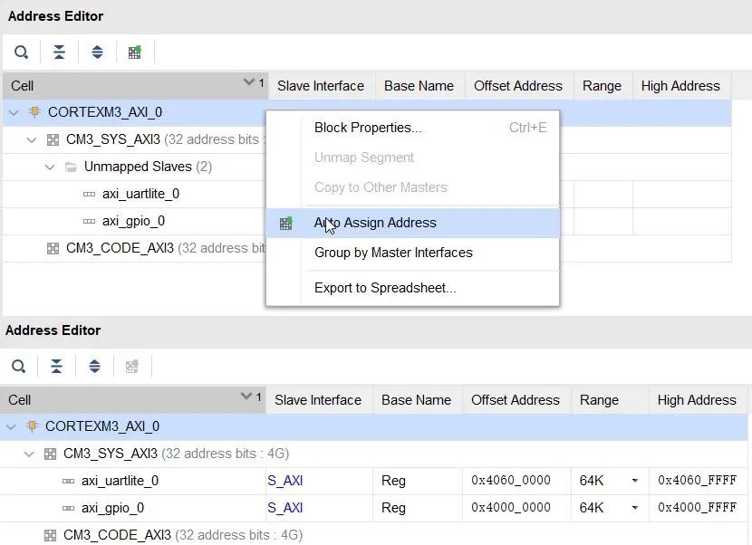
Figure 23 Base Address Allocation
After allocation, use the design validation (Validate Design) function to check the legality of the current Block Design connections.
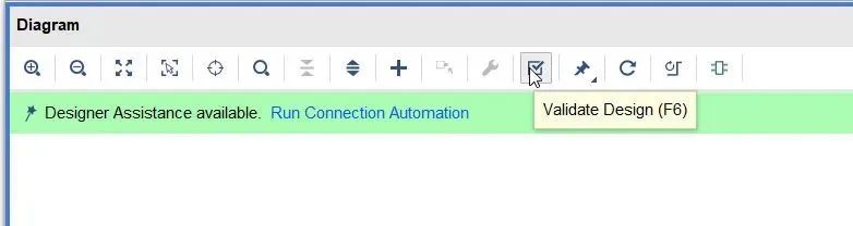
Figure 24 Validate Design
5.8 Generate Wrapper and Instantiate to Top Level
To facilitate the subsequent addition of custom FPGA logic modules, we will instantiate the Cortex-M3 soft core processor as a processor in the top-level design.
Right-click on the Block Design source file, first select Generate Output Products, wait patiently for the generation to complete, and then select Create HDL Wrapper.
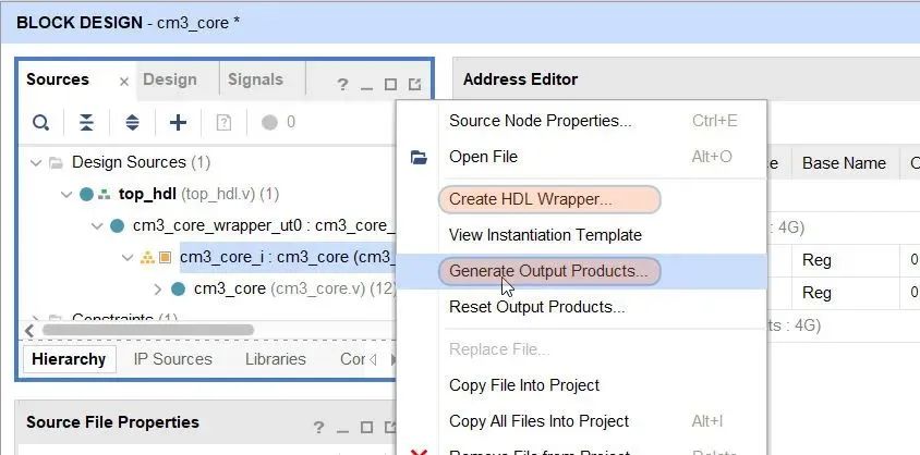
Figure 25 Generate Wrapper
Then a _wrapper Verilog file will be generated.
Create a top-level file top_hdl.v and save it in the rtl folder, instantiate the _wrapper to the top level.
module top_hdl( //Inputs input clk, input rst_n, input swclk, input uart_rxd, input [3:0] sw, //Outputs output [3:0] led, output uart_txd, //Inouts inout swdio);cm3_core_wrapper cm3_core_wrapper_ut0( //Inputs .cm3_clk(clk), .cm3_resetn(rst_n), .cm3_gpio_in_tri_i(sw[3:0]), .cm3_swclk(swclk), .cm3_uart_rxd(uart_rxd), //Outputs .cm3_gpio_out_tri_o(led[3:0]), .cm3_uart_txd(uart_txd), //Inouts .cm3_swdio(swdio));endmodule //top_hdl end5.9 Pin Allocation
After synthesis is complete, use Vivado’s graphical tool for pin allocation, especially noting to lead SWDIO and SWDCLK to the pin header for subsequent use of external Jlink debugger for Arm program downloading.
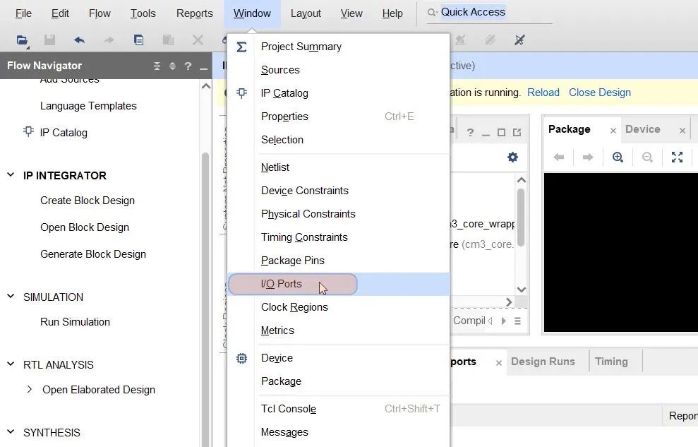
Figure 26 Pin Allocation
Alternatively, you can directly create an XDC file and use constraint statements for pin allocation.
Some constraint statements:
set_property PACKAGE_PIN R4 [get_ports clk]set_property PACKAGE_PIN V13 [get_ports swclk]set_property PACKAGE_PIN V14 [get_ports swdio]set_property PACKAGE_PIN E14 [get_ports uart_rxd]set_property PACKAGE_PIN D17 [get_ports uart_txd]set_property PACKAGE_PIN U7 [get_ports rst_n]set_property PACKAGE_PIN V9 [get_ports {led[3]}]set_property PACKAGE_PIN Y8 [get_ports {led[2]}]set_property PACKAGE_PIN Y7 [get_ports {led[1]}]set_property PACKAGE_PIN W7 [get_ports {led[0]}]set_property PACKAGE_PIN T4 [get_ports {key[3]}]set_property PACKAGE_PIN T3 [get_ports {key[2]}]set_property PACKAGE_PIN R6 [get_ports {key[1]}]set_property PACKAGE_PIN T6 [get_ports {key[0]}]If your board is the same as mine (ZYBO), then you can directly use the above pin constraints.
If the clock pin you allocated is not a global clock pin of the FPGA, you need to add a BUFG primitive for buffering.
5.10 Bitstream File Generation and Download
My board uses QSPI Flash. To improve download and startup speed, when generating the Bitstream, configure the generation options: data compression, 50M read speed, and 4-bit data line.
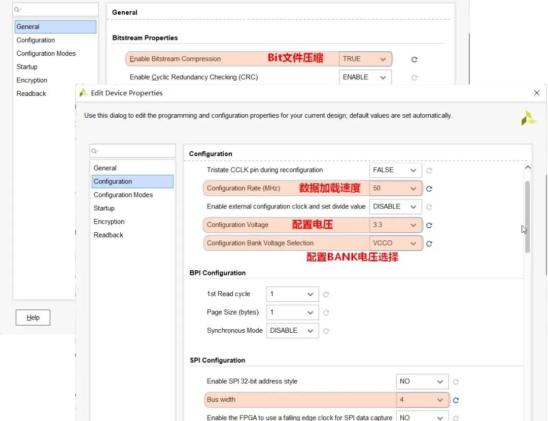
Figure 27 Bitstream Generation Configuration
Alternatively, you can directly use XDC statements for constraints:
set_property BITSTREAM.GENERAL.COMPRESS TRUE [current_design]set_property BITSTREAM.CONFIG.CONFIGRATE 50 [current_design]set_property CONFIG_VOLTAGE 3.3 [current_design]set_property CFGBVS VCCO [current_design]set_property BITSTREAM.CONFIG.SPI_BUSWIDTH 4 [current_design]The above constraints are not mandatory, they are just to improve download and configuration speed.
Wait patiently for the project synthesis to complete, generating the Bitstream file. The synthesis speed is related to the processor’s main frequency and core count.
Like the conventional FPGA downloading method, download the generated soft core Bit file to the FPGA internal using the Xilinx downloader, but do not burn it to the external SPI Flash yet.
5.11 Jlink Connection Test
After downloading, the FPGA now runs a soft core processor based on Arm Cortex-M3. You can connect to the chip using debugging tools like Jlink.
Connect the SWCLK and SWDIO of the Jlink debugger to the pins V13 and V14 we allocated.
If you do not have Jlink, you can also refer to previous articles to make your own Jlink-OB!
Step-by-step guide to making a Jlink-OB debugger
To use Keil to develop the DesignStart Cortex-M3 soft core program, you need to install a device package specifically for DesignStart.
The download link is as follows:
https://keilpack.azureedge.net/pack/Keil.V2M-MPS2_DSx_BSP.1.1.0.packOpen an STM32 Keil project, change the device to the Arm DS_CM3 we just installed, and in the Option->Debug-Setting interface, select SWD mode. The first connection will prompt you to select a device, choose Cortex-M3:
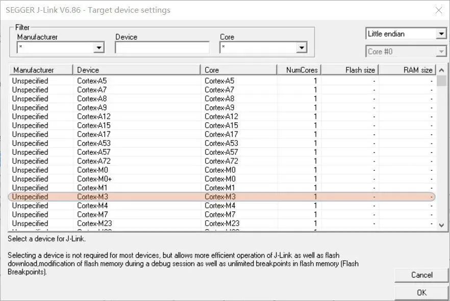
Figure 28 Select Device Model
If the above configurations are correct, you will see the connected Arm Cortex-M3 core. If not, it indicates that the FPGA project configuration has errors, and you need to verify if it is consistent with the above configuration process.
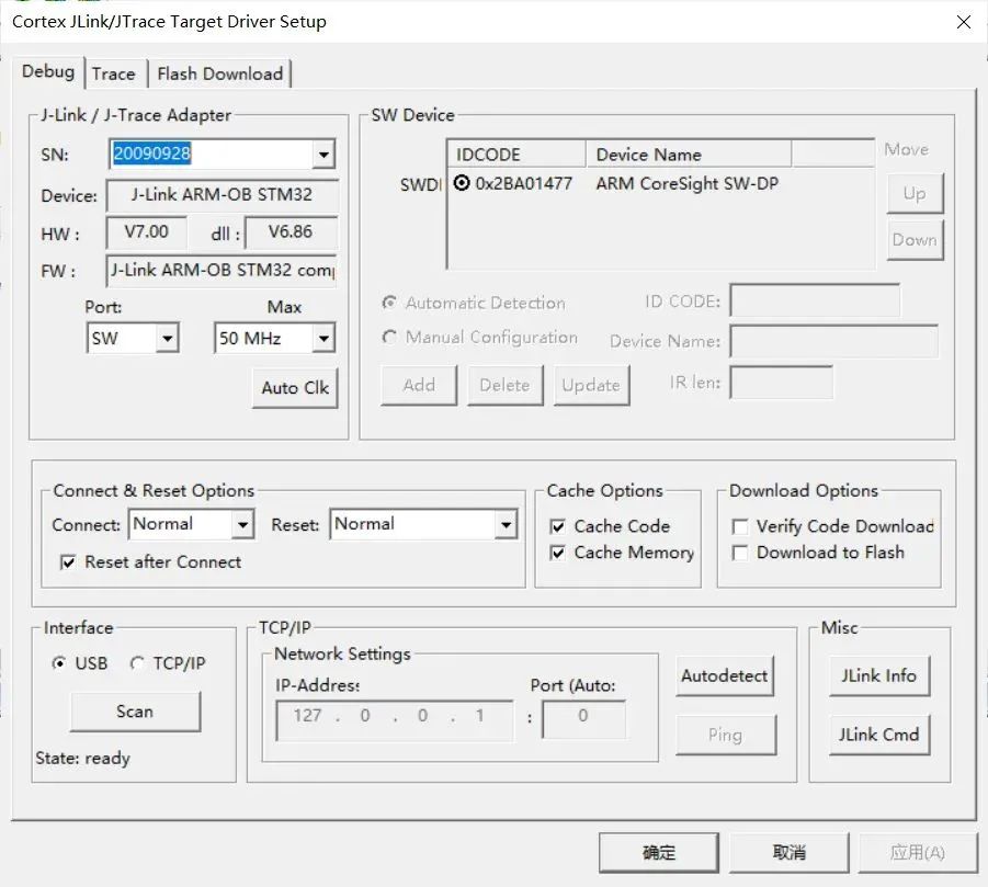
Figure 29
Once connected to the Arm core, the basic setup of the Arm Cortex-M3 soft core is finished, and we will now use Keil to write the program for the Arm core, implementing GPIO and UART control.
6 Cortex-M3 Soft Core Program Design
Similar to the conventional development process of Arm Cortex-M3 core microcontrollers, use Keil to create a new project, source files, and based on the peripheral user manual, read and write specified registers to achieve GPIO control and UART data writing, compile, download, and debug.
In the folder cortex_m3_on_xc7a100t created earlier, create a folder named mdk_prj to save the Keil-MDK project, and create the following 3 folders:
application // User source filesobject // Compiled filesproject // Keil project files6.1 Create Keil Project
Open Keil-MDK, select Project->New Project, create a project named ds_cm3_prj, and save it in the project directory.
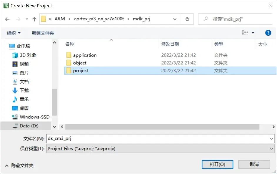
Figure 30 Keil Project Directory
Select the device model as the Arm Cortex-M3 DS_CM3 core we just installed.
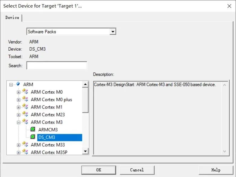
Figure 31 Select Device Model
In the component management interface, add CMSIS core files and startup files:
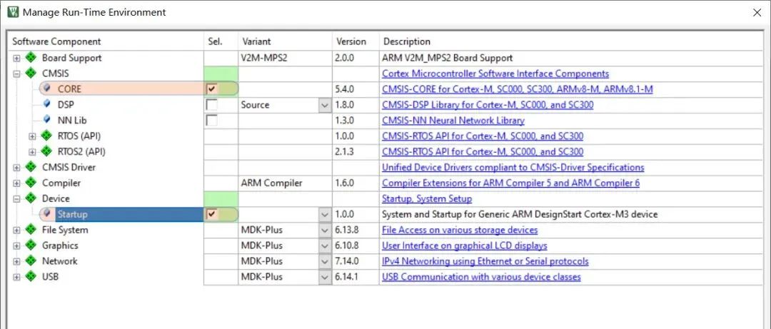
Figure 32 Add Core Files
And organize the files according to the structure shown below:
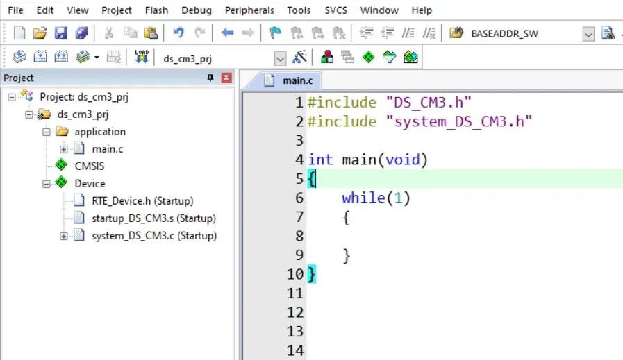
Figure 33 File Structure
6.2 Set RAM and ROM Addresses
In the project options, set the starting address of the on-chip ITCM to 0x0 and size to 64K, and the starting address of the on-chip DTCM to 0x20000000 and size to 64K:
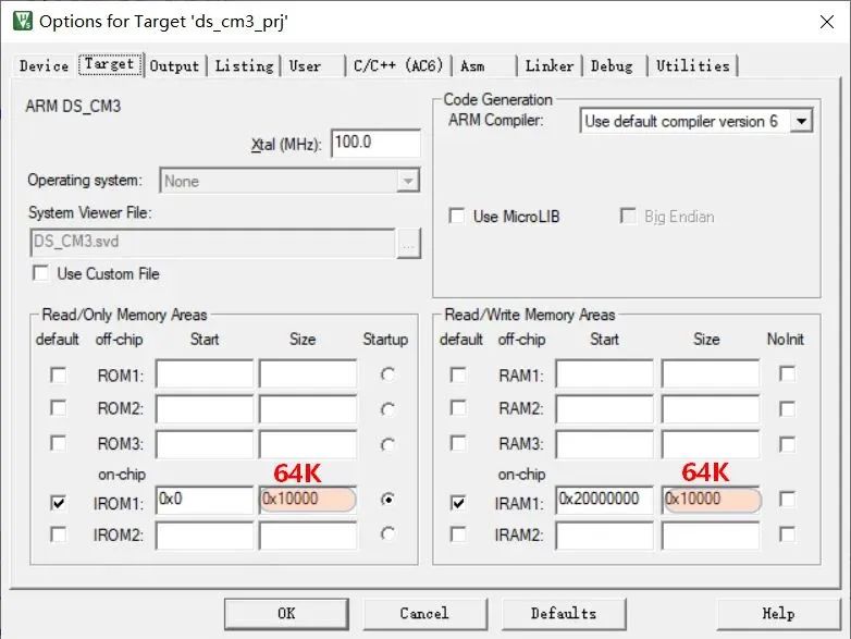
Figure 34 RAM Address Configuration
The starting addresses come from the system memory address mapping in the user manual. You can see the starting addresses of ITCM and DTCM:
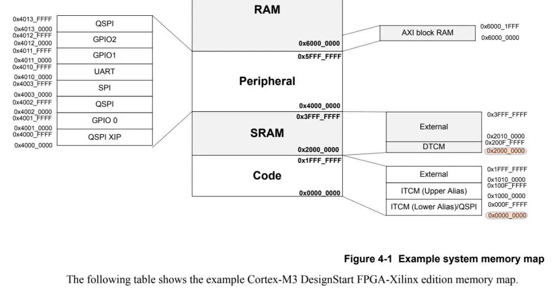
Figure 35 ITCM and DTCM Starting Addresses
The sizes are set in the Cortex-M3 core configuration:
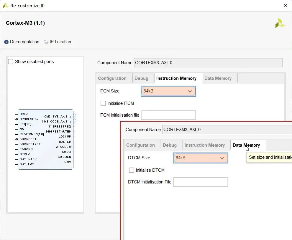
Figure 36 ITCM and DTCM Sizes
After setting, create a main.c file, enter the following content, and compile the project; it should compile without errors.
#include "DS_CM3.h"#include "system_DS_CM3.h"int main(void){ while(1) { }}6.3 GPIO Input and Output Control
By checking the AXI GPIO user manual, the data register offset address for channel 1 is 0, and the data register offset address for channel 2 is 0x08. According to the connections in Vivado, the LED is connected to channel 1, and the button is connected to channel 2, so we only need to read and write these two register addresses to control the LED and read the status of the switch.
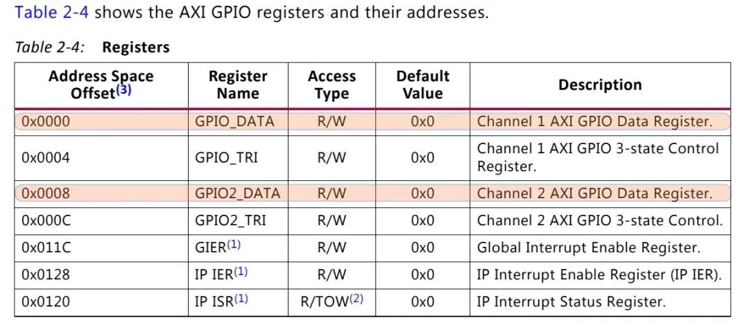
Figure 37 AXI GPIO Register Definition
In the Vivado address allocation interface, you can see that the base addresses for GPIO and UART are 0x4000_0000 and 0x4060_0000 respectively.
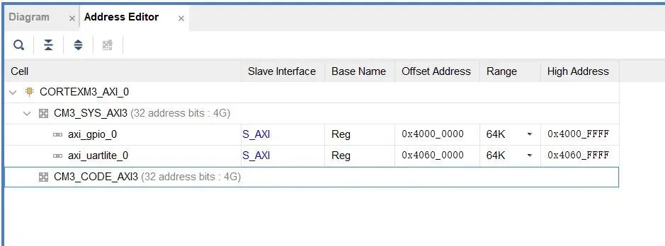
Figure 38 Peripheral Base Addresses
Control for LEL and reading the switch:
*(volatile uint32_t *) (0x40000000 + 0x0) = 0x0f; // Write 1 to the lower 4 bits of GPIO channel 1*(volatile uint32_t *) (0x40000000 + 0x0) = 0x00; // Write 0 to the lower 4 bits of GPIO channel 1uint32_t sw = 0;sw = *(uint32_t *) (0x40000000 + 0x08); // Get the 32-bit input status of GPIO channel 26.4 Serial Data Sending and Receiving
To send a byte of data to the serial port, write it into the FIFO:
while((*(volatile uint32_t *)(0x40600000 + 0x08)) & 0x08 != 0x08); // Wait for the transmit FIFO not to be full*(volatile uint32_t *) (0x40600000 + 0x04) = 0x41; // Write character 'A' = 0x41 to the transmit FIFOTo receive a byte of data from the serial port:
uint8_t dat = 0;if((*(volatile uint32_t *)(0x40600000 + 0x08)) & 0x01 == 1) // There is data in the receive FIFO dat = (*(volatile uint32_t *)(0x40600000 + 0x00)); // Read 1 byte of data from the receive FIFO.6.5 Delay Function Implementation
To make the LED changes visible to the human eye, we need to use a delay function to delay the on and off.
Use the system tick timer to implement a delay function:
volatile uint32_t cnt = 0; // volatile typevoid SysTick_Handler(void){ cnt++;}void delay_ms(uint32_t t){ cnt = 0; while(cnt - t > 0);}To ensure the delay function works accurately, we also need to change the system clock frequency in the project to match the clock configured in the FPGA.
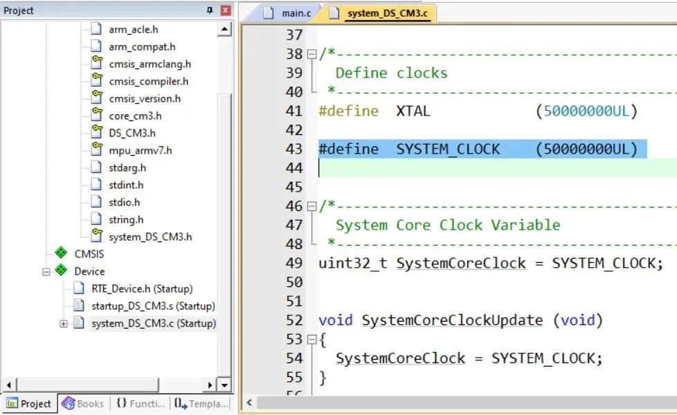
Figure 39 System Clock
The content of the completed main.c file:
#include "DS_CM3.h"#include "system_DS_CM3.h"// C library#include <stdarg.h>#include <string.h>#include <stdio.h>#define BASEADDR_LED 0x40000000#define BASEADDR_UART 0x40600000#define CHANNEL_LED 1#define CHANNEL_SW 2#define XGPIO_CHAN_OFFSET 8#define XGpio_WriteReg(BaseAddress, RegOffset, Data) Xil_Out32((BaseAddress) + (RegOffset), (uint32_t)(Data))#define XGpio_ReadReg(BaseAddress, RegOffset) XGpio_In32((BaseAddress) + (RegOffset))#define XUL_TX_FIFO_OFFSET 4 /* transmit FIFO, write only */#define XUL_STATUS_REG_OFFSET 8 /* status register, read only */#define XUL_SR_TX_FIFO_FULL 0x08 /* transmit FIFO full */#define XUartLite_GetStatusReg(BaseAddress) XUartLite_ReadReg((BaseAddress), XUL_STATUS_REG_OFFSET)#define XUartLite_ReadReg(BaseAddress, RegOffset) XGpio_In32((BaseAddress) + (RegOffset))#define XUartLite_IsTransmitFull(BaseAddress) \\ ((XUartLite_GetStatusReg((BaseAddress)) & XUL_SR_TX_FIFO_FULL) == \\ XUL_SR_TX_FIFO_FULL)#define XUartLite_WriteReg(BaseAddress, RegOffset, Data) Xil_Out32((BaseAddress) + (RegOffset), (uint32_t)(Data))volatile uint32_t cnt = 0;void SysTick_Handler(void){ cnt++;}void delay_ms(uint32_t t){ cnt = 0; while(cnt - t > 0);}uint32_t XGpio_In32(uint32_t Addr){ return *(volatile uint32_t *) Addr;}void Xil_Out32(uint32_t Addr, uint32_t Value){ volatile uint32_t *LocalAddr = (volatile uint32_t *)Addr; *LocalAddr = Value;}uint32_t XGpio_DiscreteRead(uint32_t Addr, uint8_t Channel){ return XGpio_ReadReg(Addr, (Channel - 1) * XGPIO_CHAN_OFFSET);}void XGpio_DiscreteWrite(uint32_t Addr, uint8_t Channel, uint32_t Data){ XGpio_WriteReg(Addr, (Channel - 1) * XGPIO_CHAN_OFFSET, Data);}void XUartLite_SendByte(uint32_t BaseAddress, uint8_t Data){ while (XUartLite_IsTransmitFull(BaseAddress)); XUartLite_WriteReg(BaseAddress, XUL_TX_FIFO_OFFSET, Data);}void cm3_print(const char *ptr){ while (*ptr != (char)0) { XUartLite_SendByte(BASEADDR_UART, *ptr); ptr++; }}void MyUartPrintf(char *fmt,...){ unsigned char UsartPrintfBuf[296]; va_list ap; unsigned char *pStr = UsartPrintfBuf; va_start(ap, fmt); vsnprintf((char *)UsartPrintfBuf, sizeof(UsartPrintfBuf), (const char *)fmt, ap); va_end(ap); while(*pStr != 0) { XUartLite_SendByte(BASEADDR_UART, *pStr); pStr++; }}void led_blink(void){ XGpio_DiscreteWrite(BASEADDR_LED, CHANNEL_LED, 0); delay_ms(500); XGpio_DiscreteWrite(BASEADDR_LED, CHANNEL_LED, 0xf); delay_ms(500);}int main(void){ uint32_t sw = 0; SystemCoreClockUpdate(); SysTick_Config(SystemCoreClock / 1000); cm3_print("Hello DesignStart ARM Cortex-M3 on FPGA Xilnx Artix-7 XC7A100T \r\n"); MyUartPrintf("SystemCoreClock = %ld\r\n", SystemCoreClock); while(1) { led_blink(); sw = XGpio_DiscreteRead(BASEADDR_LED, CHANNEL_SW); MyUartPrintf("key state = %d-%d-%d-%d\r\n", sw >> 3, sw >> 2 & 1, sw >> 1 & 1, sw & 1); }}The implemented functions are that 4 LEDs blink every 100ms, while the serial port outputs the real-time status of the switch.
After compiling without errors, you can proceed to program downloading.
6.6 Flash Programming Algorithm Generation
To use Jlink to download the program, you need to specify the Flash programming algorithm, but the algorithms that come with Keil do not include what we need:
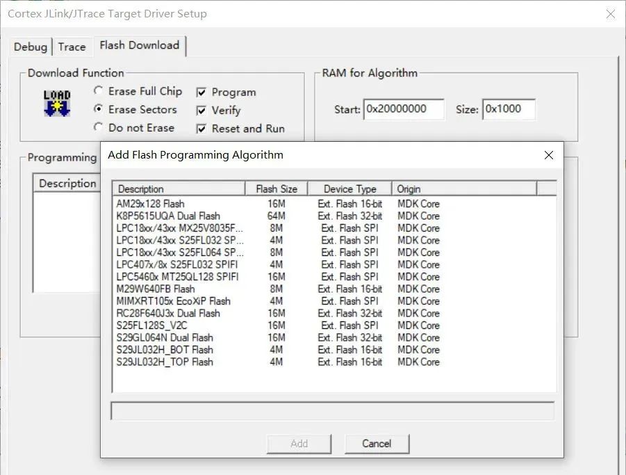
Figure 40 Download Algorithm
Therefore, we need to customize a Flash programming algorithm. Open the \\Arm\\Flash folder in the Keil installation directory, copy the _Template folder, and rename it to DS_CM3.
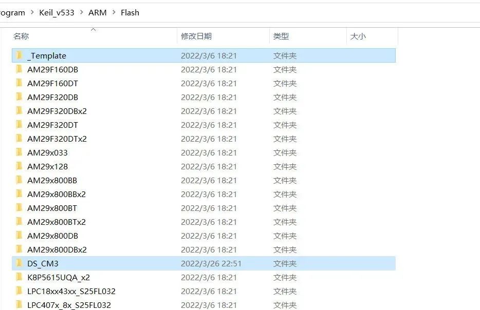
Figure 41 Copy Template
Open the Keil project inside:
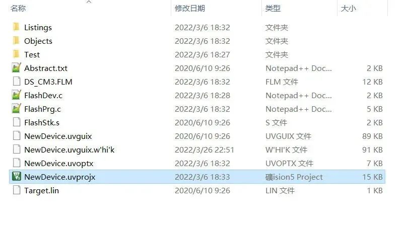
Figure 42 Download Algorithm
This project allows you to set the Flash starting address, size, erase size, etc.
Fill in the FlashDev.c file with the following content, keeping consistent with our previous ITCM configuration, starting address 0x0, size 64K:
#include “..\FlashOS.H” //FlashOS Structures
#include "..\FlashOS.H" // FlashOS Structuresstruct FlashDevice const FlashDevice = { FLASH_DRV_VERS, // Driver Version, do not modify! "MyCM3onFPGA", // Device Name ONCHIP, // Device Type 0x00000000, // Device Start Address 0x00010000, // Modify to 64KB 1024, // Programming Page Size 0, // Reserved, must be 0 0xFF, // Initial Content of Erased Memory 100, // Program Page Timeout 100 mSec 3000, // Erase Sector Timeout 3000 mSec // Specify Size and Address of Sectors 0x010000, 0x000000, // Only one sector, starting address is 0 SECTOR_END};In the FlashPrg.c file, implement some functions for erasing the storage area:
#include "..\FlashOS.H" // FlashOS Structures#include "string.h"int Init (unsigned long adr, unsigned long clk, unsigned long fnc) { return (0); // Finished without Errors}int UnInit (unsigned long fnc) { return (0); // Finished without Errors}int EraseChip (void) { memset((unsigned char *)0, 0, 0x10000); return (0); // Finished without Errors}int EraseSector (unsigned long adr) { memset((unsigned char *)adr, 0, 1024); return (0); // Finished without Errors}int ProgramPage (unsigned long adr, unsigned long sz, unsigned char *buf) { memcpy((unsigned char *)adr, buf, sz); return (0); // Finished without Errors}After compiling without errors, a FLM file will be generated in the project directory.

Figure 43 Newly Generated Download Algorithm
Copy it to the upper directory:
Figure 44 Newly Generated Download Algorithm
6.7 Compile, Download, and Run
Then open our Arm core Keil project and add the DS_CM3 Flash programming algorithm:
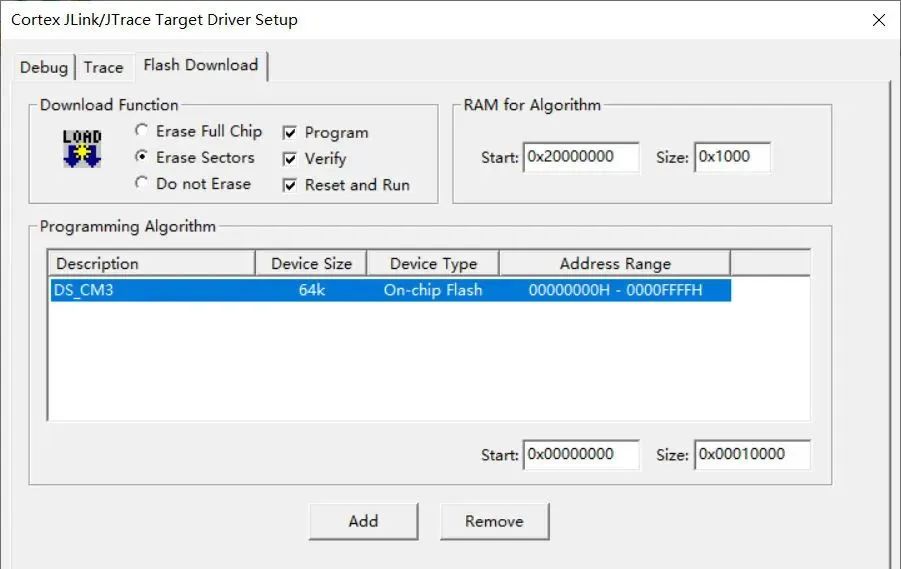
Figure 45 Add Flash Programming Algorithm
Click the download button to download the Arm program to the Arm core:
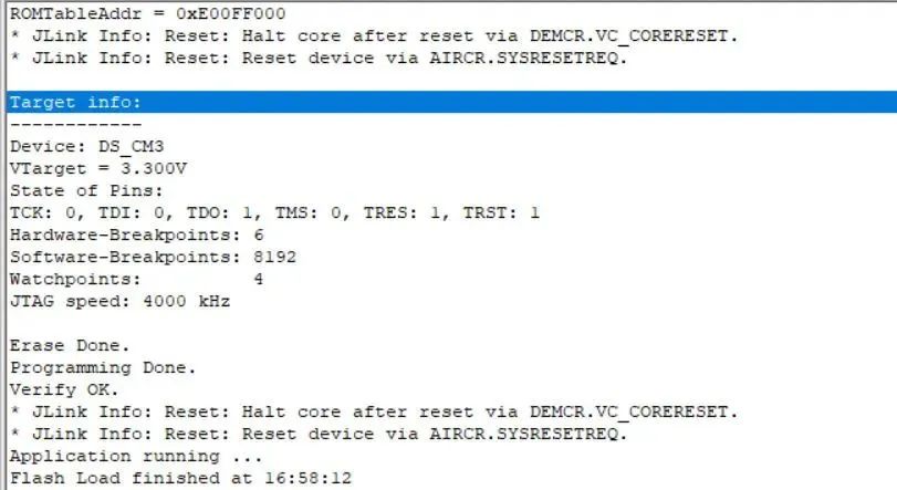
Figure 46
You can see that the LED blinks every 500ms, and the serial data is output every 1s. At the same time, pressing the button will output the status of the button through the serial port.
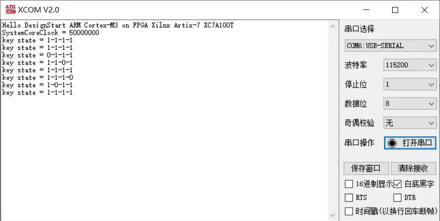
Figure 47
Like other Arm core chips, it also supports online debugging:
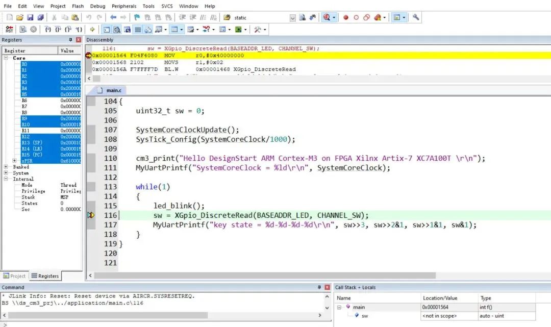
Figure 48
Since the Arm program is downloaded to the RAM storage area of the Cortex-M3 soft core, it will be lost after power off. How to download the program to the external SPI Flash, I have not successfully implemented yet.
Recommended Reading
-
Deep Review of ZYNQ Development Board: A Powerful Combination of High-Performance FPGA and Dual-Core Arm!
-
FPGA Automation Execution in Linux
-
Overview of FPGA Smart Network Cards (1): PISA + Rocket


Long press to recognize the QR code to add the Miss Jishu WeChat (aijishu20), and join the Arm Technology Academy reader group.
3100+ courses using 11 Arm educational kits are available for free download, including embedded systems, chip design, signal processing, operating systems, etc.
Follow Arm Technology Academy
 Click below “Read the original text“, to download the Arm educational kit for learning and charging immediately.