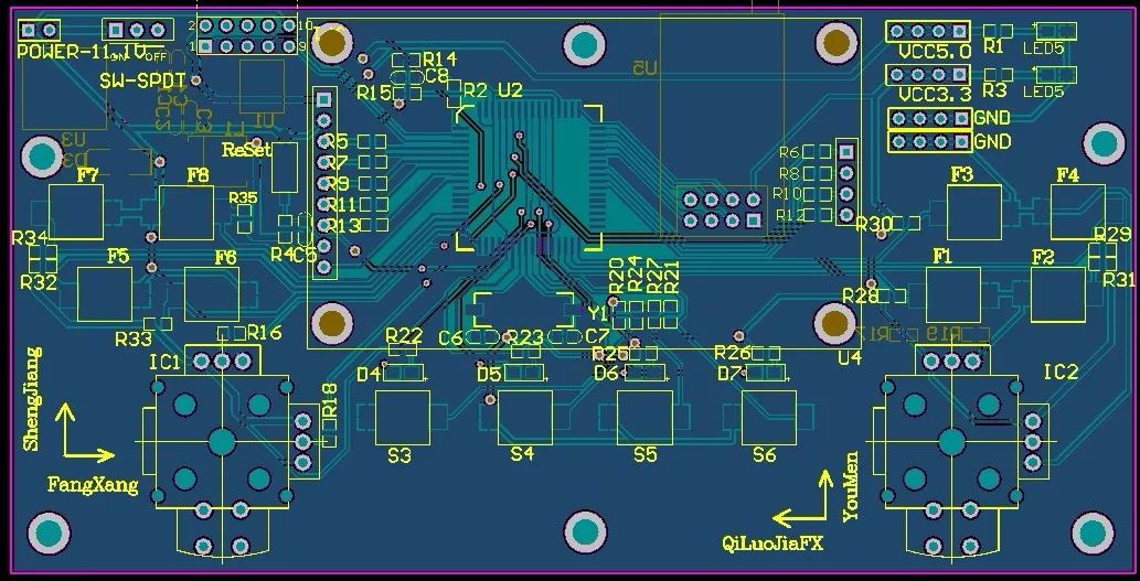
When passing the PCB schematic to the layout design, there are six key considerations. All examples mentioned are developed using the Multisim design environment, but the same concepts apply when using different EDA tools!

When transferring the schematic to the layout environment via the netlist file, device information, netlist, layout information, and initial trace width settings are also conveyed.
Here are some recommended steps to prepare for the layout design phase:
1. Set the grid and units to appropriate values. To achieve more precise layout control for components and traces, set the component grid, copper fill grid, via grid, and SMD grid to 1 mil.
2. Set the blank area of the PCB outline and the vias to the required values. PCB manufacturers may have specific minimum or nominal recommended values for blind and buried vias.
3. Set the appropriate pad/via parameters according to the capabilities of the PCB manufacturer. Most PCB manufacturers can support smaller vias with a drill diameter of 10 mil and a pad diameter of 20 mil.
4. Set design rules according to requirements.
5. Set custom shortcuts for commonly used layers to quickly switch layers (and create vias) during routing.
Handling Errors During Schematic Transfer
A common error during schematic transfer is the absence or incorrect assignment of package footprints. It is important to note:
If there is a device in the schematic without a footprint, a warning message will pop up indicating that the virtual component cannot be exported. In this case, no default footprint information will be passed to the layout, and the component will simply be removed from the layout.
If the footprint is passed over but does not correctly match a valid footprint shape, a warning message indicating a mismatch will also occur during the transfer.
Correct the footprint assignment in the schematic or create a valid footprint for any device. After correction, execute the forward annotation step to update and synchronize the design information.
Updating Design Through Annotation
Annotation is the process of transferring design changes from the schematic to the layout or from the layout to the schematic. Backward annotation (layout to schematic) and forward annotation (schematic to layout) are key to maintaining design accuracy.
To protect completed work, it is necessary to back up and archive the current version of the schematic and layout files before any important forward or backward annotation steps.
Do not attempt to make changes in both the schematic and layout simultaneously. Only make changes to one part of the design (either the schematic or the layout) and then execute the correct annotation steps to synchronize the design data.
Renumbering Components
Renumbering components refers to the function of renumbering elements on the PCB in a specific sequence. Reference designators should be sorted from top to bottom and left to right on the PCB. This makes it easier to locate components on the board during assembly, testing, and troubleshooting.
Handling Last-Minute Changes to Components or Netlists
Last-minute changes to PCB components or netlists are undesirable, but sometimes must be made due to component availability issues or last-minute design errors. If the changes involve components or netlists, they should be made in the schematic and then passed to the layout tool through forward annotation.
Here are some tips:
1. If a new component (like a pull-up resistor on an open-drain output) is added after the layout design has started, add the resistor and network from the schematic. After forward annotation, the resistor will appear as an unplaced component outside the PCB outline, with a flying wire indicating the connection network. Next, move the component inside the PCB outline and perform normal routing.
2. Backward annotation and reference designator changes can work well together, such as renumbering after layout.
Highlighting to Locate Components
During the PCB layout process, one way to browse specific components or traces in the schematic is to use the ‘Highlight Selection’ feature. This feature allows you to select a component or a trace (or multiple objects) and see their location in the schematic.
This feature is particularly useful when matching bypass capacitors and their corresponding IC connections. Conversely, it can also be used to locate specific components or traces in the layout while browsing the schematic.


Source: JXPCA
Copyright notice: The above images and text are copyrighted by the original author. The “Meizhou Printed Circuit Industry Association” shares this as a reprint. If there are any copyright issues, please contact us for removal.