“This article presents a novel process based on TPL, combined with the CWI development system, successfully fabricating embedded microfluidic chips with channel sizes reaching 30 μm and complex structures, enabling functions such as droplet generation and efficient cell sorting. This technology is expected to significantly enhance the resolution, compactness, and customization capabilities of microfluidic devices, empowering a new generation of biological detection and diagnostic platforms..””
∇∇
01『Experimental Background』
Microfluidic chips are widely used in analytical chemistry and molecular biology due to their advantages of low reagent consumption, high integration, and sensitivity.
In recent years, additive manufacturing (3D printing) technology has entered the microfluidic field, especially Two-Photon Lithography (TPL), which provides true three-dimensional construction capabilities for microfluidic chips with sub-hundred-nanometer high resolution, breaking the limitations of traditional 2D or 2.5D processes.
02『Overview of the Solution』
A manufacturing solution for microfluidic chips has been proposed, combining high-resolution Two-Photon Lithography (TPL) with chip-external interface (CWI), successfully addressing issues such as limited channel sizes, difficult cleaning, and long preparation cycles in traditional microfluidic manufacturing.
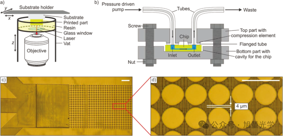
The key innovations of the solution include:
-
Integrated Embedded Microfluidic Structure Printing: Achieving high-resolution structures from microns to nanometers (minimum channel width of 30 μm, structural features of 4 μm) through TPL, supporting complex 3D channel configurations;
-
Breaking Traditional Material Limitations: Successfully using high-viscosity resins (such as UpFlow) for printing and developing microchannels, breaking the dependency on low-viscosity resins (such as PEGDA);
-
Building an Efficient “Development Interface” System: By coordinating the CWI structure with a pressure pump, the developer solution is directed into the microchannels, effectively removing uncured resin, with a maximum pressure of 6.9 bar and no leakage;
-
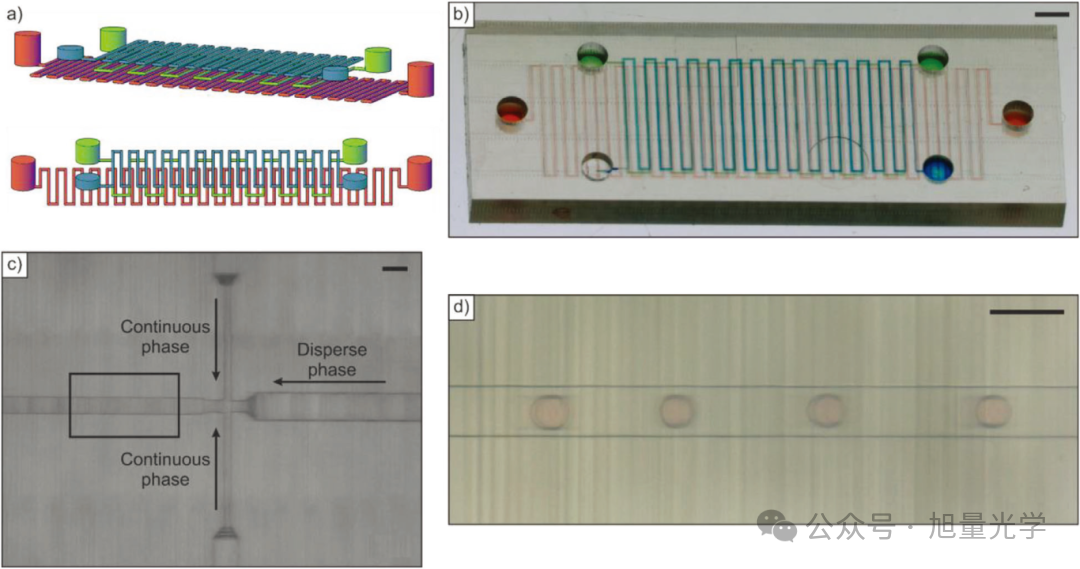
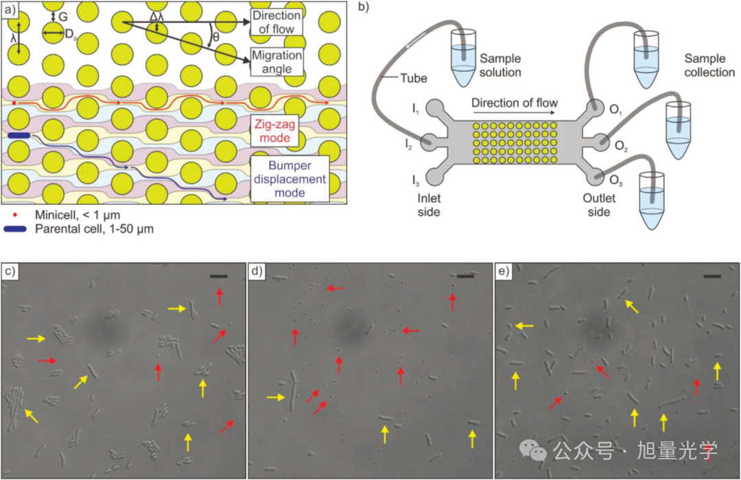
Modular Application Demonstration: Constructing serpentine channels, droplet generators, and DLD cell sorting chips, demonstrating the technology’s wide applicability in high-density channels, two-phase flow control, and microbial manipulation.
03『Experimental Setup and Methods』
✦ Printing System and Material Selection
(1) Using a two-photon 3D printing system, equipped with a 10× objective lens and a 1 W femtosecond laser (90 fs pulse width, 780 nm), supporting high-speed scanning (up to 1000 mm/s), with a printing throughput of up to 200 mm³/h;
(2) The photoresists used include:
-
UpFlow (viscosity up to 555 mPa·s) for structuring sub-100 μm channels;
-
UpPhoto for cell chips, featuring fluorescent properties for easy detection of cleaning effects.
✦ Printing Configuration and Direction Control
(1) Flexibly adjusting the printing direction based on structural size and resolution requirements:
-
Horizontal printing for high planar resolution needs (e.g., DLD chips);
-
Vertical printing for fine Z-direction feature structures;
(2) Using a 10× objective lens (NA 0.4), achieving an XY resolution of 0.73 μm and a Z-direction resolution of 9.2 μm.
✦ Chip-External Interface (CWI) System Development Process
(1) Independently designing a 3D printed CWI module, including:
-
Upper Part: Equipped with a clamping mechanism and ports;
-
Lower Part: Grooves aligned with channel inlets and outlets;
(2) After embedding the microfluidic chip into the CWI structure, it is fixed with screws and pressurized, using a pressure pump to inject the developer solution (IPA or PGMEA) at 6.9 bar pressure to ensure the uncured material is thoroughly washed away;
(3) Strong interface compatibility (using standard HPLC connectors), reusable, adaptable to various chip experimental needs.
✦ Performance Testing and Function Verification
(1) Development Performance Testing: Conducting development experiments on different channel diameter/length combinations, establishing a “pressure drop – developability” relationship table;
(2) Surface Morphology Testing: Measuring channel roughness using a white light interferometer, with Ra as low as 8.6 nm;
(3) Functional Demonstration Modules include:
-
Serpentine Channel Chip: Three-layer structure, with the longest channel reaching 20 cm;
-
Droplet Generator: Controls the formation of 45 μm droplets;
-
DLD Cell Sorting Chip: Minimum critical diameter of 800 nm, inter-column spacing of 4 μm, sorting efficiency of up to 89.4%.
04『Experimental Results』
The research successfully fabricated high-precision embedded microfluidic chips with a minimum channel diameter of 30 μm and a roughness as low as 8.6 nm through two-photon lithography combined with pressure-assisted development. Utilizing a 6.9 bar development scheme, it overcame the cleaning challenges of high-viscosity resins.
In terms of function verification, three-layer serpentine channels, droplet generators, and cell sorting chips were printed, achieving a compact layout of a 20 cm long channel, stable generation of 45 μm droplets, and efficient separation of small cells (with an efficiency of 89.4%). The results indicate that this solution possesses high resolution, strong compatibility, and significant application scalability, suitable for rapid manufacturing of complex microfluidic systems.
05『Experimental System Reference』
Our system serves as an integrated platform with true research-grade nano-manufacturing capabilities, not only meeting critical technical needs in experiments but also achieving breakthroughs and leadership in multiple dimensions.
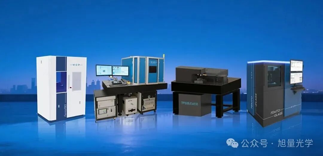
Our TPP nano-printing system features:
-
Ultra-high precision: 30 nm resolution (after shrinkage), breaking the optical diffraction limit
-
Multi-material compatibility: Supports over 20 materials including metals, semiconductors, and biomaterials
-
Efficient parallel processing: Printing speed of up to 1000 mm³/h (10000 times faster than traditional methods)
-
Intelligent control: Fully automated CAD to printing process, supporting large-size splicing
-
Unique hydrogel technology: 1-15 times adjustable shrinkage ratio for super-resolution manufacturing
-
Complex structure capability: Can print suspended structures and high aspect ratio devices
-
Ultra-smooth surfaces: Roughness ≤ 5 nm (after shrinkage)
-
Open material platform: Compatible with customer-defined material development
-
Multi-field applications: Photonic chips, biological scaffolds, micro-nano robots, etc.
∇∇
“We provide a clear, precise, and scalable micro-nano manufacturing platform for scientific research. Research teams are welcome to collaborate on topics such as fiber processing, waveguide manufacturing, TPP printing, and more for sample cooperation, solution customization, or system consultation..”