As reported by Nextplatform, the x86 architecture took 15 years to gain a significant share in data center computing, while the Arm architecture took about 10 years to establish a measurable foothold. Perhaps the RISC-V architecture could achieve the same in just five years, as hyperscale companies and cloud builders are tired of not having more control over their infrastructure destiny than they do now.
This is undoubtedly what companies like Tenstorrent, SiFive, Esperanto Technologies, and Ventana Micro Systems are looking forward to. Given the ability and willingness of hyperscale companies and cloud builders to control their own hardware and software stacks, and their acknowledgment that they do not have to design everything down to the transistor level, we believe that companies building chiplets and licensing IP will gain some business from these data center giants to accelerate their server design cycles.
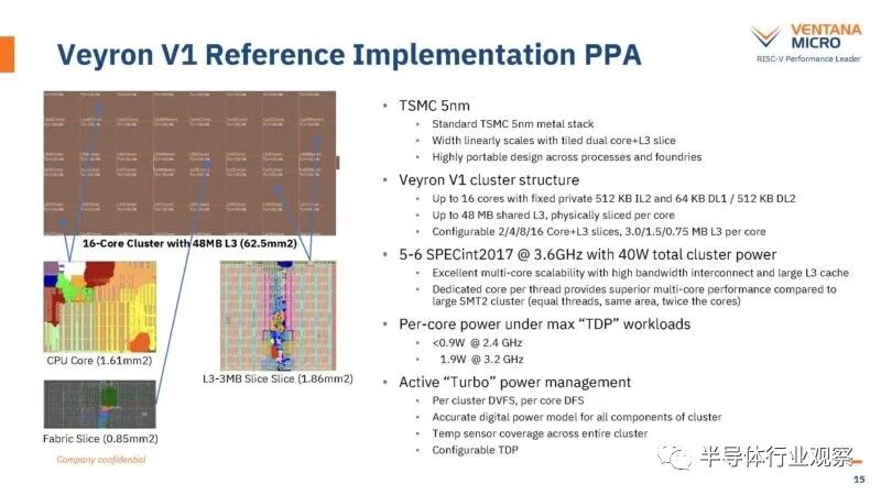
Back in December 2022, Ventana co-founder and engineer revealed the company’s VEYRON V1 server chip design, which is competitive with the then-current x86 and Arm server chips. With the Veyron V1 chiplet set to launch in the second half of this year and having been available as an FPGA emulator since last year, you might wonder why Ventana is so eager to bring the Veyron V2 to market.
The answer is that Ventana must compete with a new round of x86 and Arm server chips in the field and should seek to meet the demands of supporting hyperscale companies and cloud builders, changing its RISC-V server design’s chiplet interconnect to commit to creating RISC-V server chips.
UCIe, the Inevitable Choice for Chiplets
The shift in interconnect is a subtle but important change. The original Veyron V1 design has been in the works for two years, and Ventana chose the best option available at the time for chiplet interconnect, called Bunch of Wires, or BoW, driven by the Open Domain Specific Architecture group within the Open Compute Project. This is about as open as a standard can get, especially considering that platforms like Ampere Computing, Alibaba, AMD, ARM, Cisco Systems, Dell, Eliyan, Fidelity Investments, Goldman Sachs, Google, Hewlett Packard Enterprise, IBM, Intel, Lenovo, Meta, Microsoft, Nokia, Nvidia, Rackspace, Seagate Technology, Ventana, and Wiwynn all support BoW and are committed to establishing a fast, broad, and inexpensive chip-to-chip interconnect standard to enable the promise of heterogeneous chiplet integration across vendors and processes.
However, Intel introduced an alternative universal Chiplet Interconnect Express (or UCI-Express) standard in March 2022, which essentially enhances its own high-speed interface bus, a royalty-free PHY for connecting chiplets that was announced as early as 2018, well ahead of BoW. Because the IT industry favors technological differentiation and choice, and Intel prefers to exert more control than BoW, UCI-Express was born, much like Compute Express Link (or CXL), a standard developed by Intel for placing semantics over memory PCI-Express, which has been adopted by nearly everyone with a coherent memory competitive approach across CPUs and accelerators. UCI-Express was initially recognized by advanced semiconductor manufacturers, AMD, Arm Holdings, Intel, Google, Meta Platform, Microsoft, Qualcomm, Samsung, and TSMC. Initially, HPE, IBM, and Nvidia were missing from the original UCIe participants, but they will eventually come around.
Balaji Baktha, co-founder and CEO of Ventana, stated that in conversations with 46 current and potential customers focused on the Veyron V1 and V2 CPU designs, it became clear that UCI-Express is the best choice for chiplet interconnect. Therefore, the company accelerated the release of Veyron V2, which includes a significant number of enhancements to the RISC-V core, as it adopts UCI-Express instead of BoW for chiplet interconnect.
Here is a comparison of the feed and speed of BoW, AIB 2.0, and UCI-Express 1.1 interconnects, supplemented by a paper written by Lei Shan, who worked on interconnect hardware at IBM’s TJ Watson Research Center and now serves at Arm’s server chip newcomer Ampere Computing:
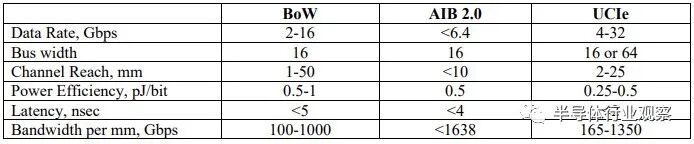
As you can see, the data rate of UCI-Express is twice that of BoW, while the bus bandwidth can be the same or up to four times higher. The channel reach is half that of UCI-Express, but the link’s energy efficiency is improved by two times, and the latency is less than half that of BoW. The bandwidth per millimeter is also 35% to 65% higher.
“There is no doubt that if chip designers want to use chiplets, they must support UCI-Express,” Baktha told The Next Platform. “There is a huge push and momentum behind UCI-Express because everyone wants a standard. BoW could have become a standard. But we do not want to be the ones to continue building that standard in the future because the UCIe standard also effectively addresses packaging costs, and the yield is at a very ideal level. UCIe also addresses the 3D memory stacking issue. So it is easy to leverage UCI-Express 2.0 and use our own expertise to fill the gaps that UCI-Express 1.0 has – for example, UCIe does not provide a link to the AMBA CHI coherent interface bus at all, so we added AMBA functionality on UCI 2.0,” Baktha continued.
Seizing Vector Extensions for High-Performance RISC-V
Another significant change that Ventana hopes to quickly seize and integrate into its Veyron V2 core design is the RISC-V Vector 1.0 512-bit vector extension, which is similar to the extension offered by Intel’s “Knights” Xeon Phi processors since 2015. This was also just added to AMD’s “Genoa” Epyc processors a year ago.
These 512-bit vector engines are not literal clones of Intel’s AVX-512 (at least in software terms, they are similar to the engines in AMD’s Genoa chips), but they are close enough that they will not create a complete software nightmare for Linux developers wanting to port their code from x86 to RISC-V using AVX-512. Additionally, the 512-bit vectors will provide performance competitive with x86 and Arm processors for HPC and AI workloads, where the CPU will perform mathematical operations rather than relying on accelerators on or off the CPU package like GPUs and other accelerators.
Ventana has added extensions to the V2 core that enable the vector engines to support matrix operations and allow customers to add their own matrix engines to the architecture, whether in the core or in discrete chiplets adjacent to it using UCI-Express links. By the way, the V1 core had no vector engines or matrix engine extensions, which would clearly be a problem as a significant amount of AI inference is still done on the CPU, and in some cases, AI training and HPC simulations and modeling are also done on the CPU.
Another major change in the Veyron V2 design is the full core name we have been discussing – to avoid confusion with Arm Ltd’s “Demeter” V2 core, which has a pair of 256-bit vectors in its Neoverse CPU design. To this end, Ventana has created a significantly improved RISC-V core.
By more aggressively fusing instruction processing in the Veyron V2 core and making a number of other adjustments, Ventana has been able to increase the instructions per clock (IPC) for a wide range of workloads by 20%. The high-end clock speed of V2 has been boosted to 3.6 GHz, while the clock speed of the Veyron V1 core was also 3 GHz, meaning that the performance from the V1 core to the V2 core in Ventana’s Veyron RISC-V CPU design has increased by 20%, resulting in an overall performance increase of 40%.
Baktha delivered a keynote speech today at the RISC-V Summit 2023 and revealed more speeds and feeds of the Veyron V2 chiplet complex and the potential CPU designs that Ventana customers can create using its intellectual property and that of other companies.
4nm Process, Supporting Up to 192 Cores
The Veyron V2 core is designed using TSMC’s 4nm process, which is a shrink of the 5nm process used in the default design of the Veyron V1 chiplet we discussed earlier this year. The V2 core supports the RVA23 architecture profile, which mandates the inclusion of the 512-bit vector extension. There are also cryptographic functions running on the vector engines.
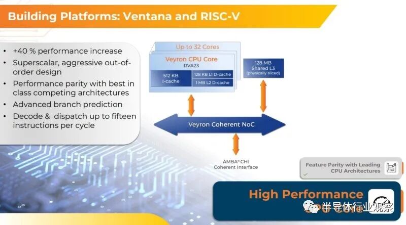
Here is a conceptual look at what a CPU based on V2 would look like, featuring an I/O chip and six 32-core V2 chiplets along with some linked domain-specific accelerators:
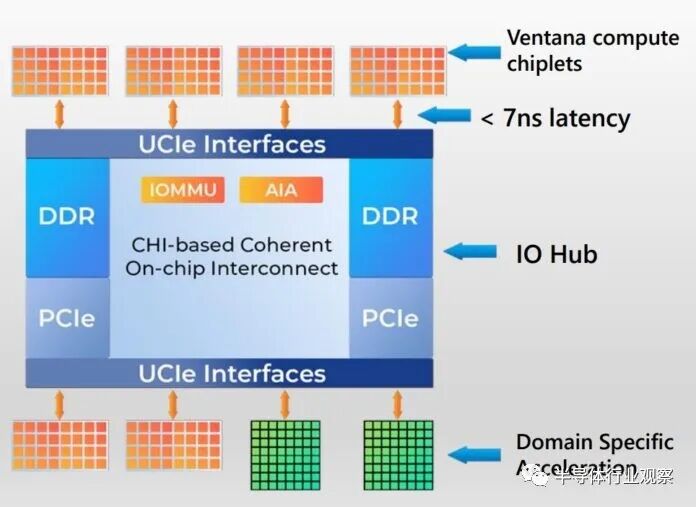
This diagram shows the I/O hub linked to PCI-Express 5.0 controllers and DDR5 memory controllers, but if the company wishes, it can replace the HBM3 memory controller. The default design has 12 DDR5 memory controllers on six V2 chiplets, or 8 DDR5 memory controllers on four V2 chiplets, which aligns with the balance we currently expect to see in any server CPU.
Ventana’s V2 core supports the RV64GC specification and implements superscalar, out-of-order pipelines that can decode and dispatch up to 15 instructions per clock cycle. Thanks to its IOMMU design and advanced interrupt architecture (AIA), the V2 core can support Type 1 and Type 2 server virtualization hypervisors as well as nested virtualization.
The core also features ports for debugging, tracing, and performance monitoring. All of these are bets for modern hyperscale data center server CPUs. Both the V1 and V2 cores do not have simultaneous hyperthreading, just like the Arm cores from Amazon Web Services and Ampere Computing do not have simultaneous hyperthreading, and the future “Sierra Forest” Xeon SP processors using the future “Sierra Glen” cores will not have this feature either.
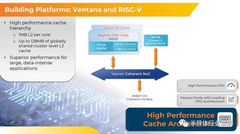
The Veyron V2 core has a 512 KB L1 instruction cache and a 128 KB L1 data cache, along with a 1 MB L2 data cache. These cores have an associated 4 MB L3 cache slice, and thus there is 128 MB of cache across the 32 cores in the Veyron V2 chiplet complex. The cores on each chiplet are interconnected using a proprietary on-chip coherent network mesh that provides 5 TB/sec of aggregate bandwidth for the cores, memory, and other I/O.
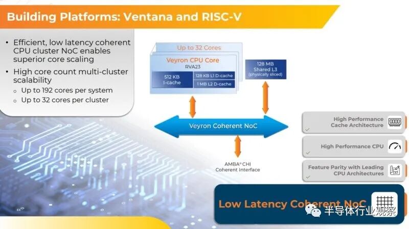
Four V2 chiplets can be interconnected with UCI-Express to create a 128-core complex, and if you really want to push the limits, you can connect up to six chiplets together to achieve 192 cores in a single Veyron socket. While its per-core performance may not reach Zen 4c levels, it focuses on UCIe and domain-specific acceleration (DSA) to provide a more modern computing platform.
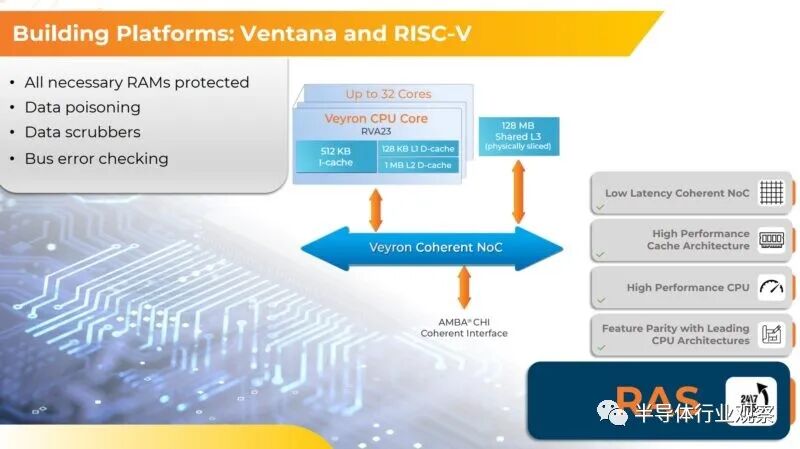
Another significant feature of the chip is RAS, with ECC capabilities, among others.
Today, data center processors need to have secure boot and authentication. Chiplet CPUs also need chiplet authentication.
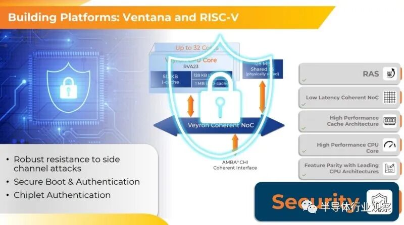
As mentioned at the beginning, Ventana uses UCIe to connect to an I/O hub with DDR and PCIe controllers. UCIe will become a force in the industry, and this diagram should help explain why. We do not see Ventana having just CPU core computing chiplets. Instead, these slides also showcase domain-specific accelerator chiplets.
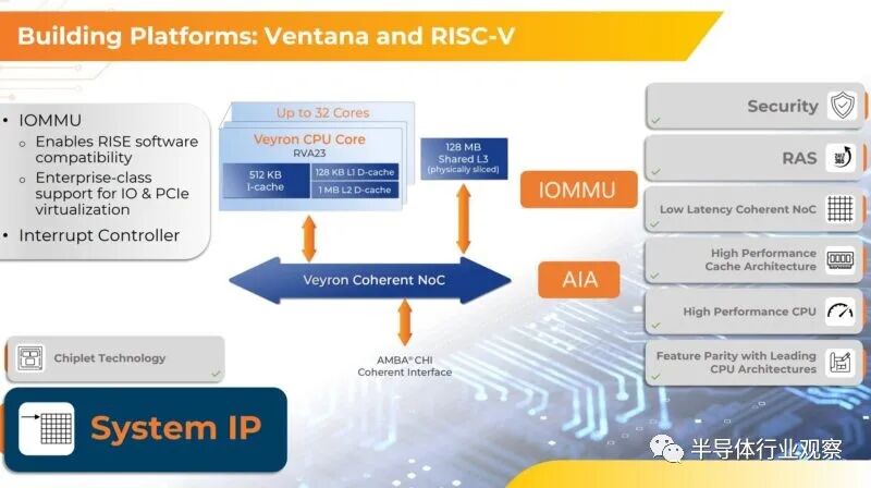
Ventana also supports RISE. RISC-V is sometimes compared to the Wild West because, theoretically, people can do anything with a CPU. Ventana is a RISC-V design, but it hopes to be a compatibility design based on standards, so RISE support is important.
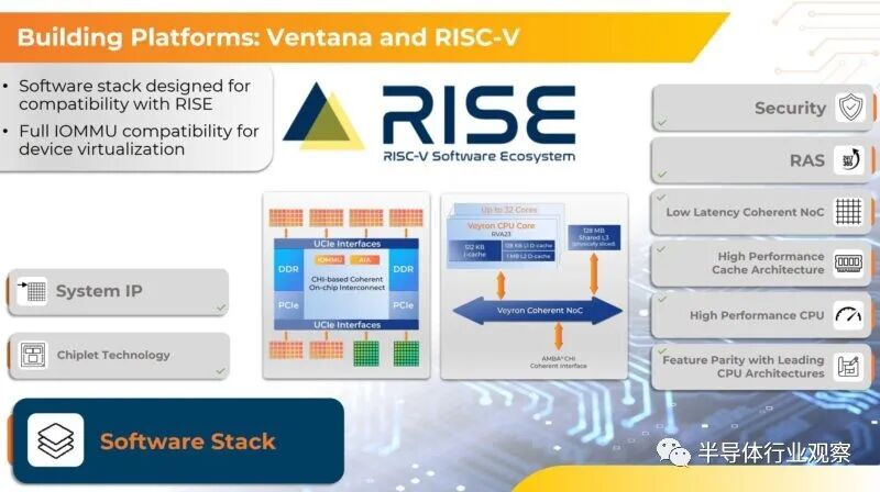
To be fair, Ventana can have good RISC-V components, but being 5% faster than alternatives in a generation will not make companies switch to the architecture. Instead, the company hopes to integrate accelerated chiplets (possibly based on UCIe) into the I/O hub as a core part of its strategy, giving its components different performance curves. For example, in storage servers, integration of encryption and compression may be important. In CDN servers, this could be a transcoding accelerator. The idea is that integrating these accelerators will change the curve. This is already industry practice; it’s just that AMD and companies like Ampere and Intel have integrated accelerators directly into CPUs on the PCIe bus.
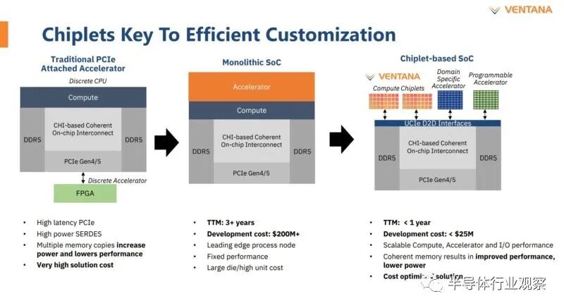
At this point, the idea of adding accelerator chiplets on the package for the 32-core UCIe-supported chiplet may sound exciting, but there’s more. Hyperscalers want to add custom acceleration directly to the I/O hub. Ventana is already promoting its chiplets for customer-designed I/O hubs.
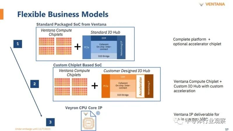
Chiplet technology is very interesting because it allows for faster chip manufacturing. FPGA can be added, and then ASIC accelerators can be added. This increases flexibility but also lowers the barrier to entry, as it allows for the use of smaller IP blocks to build packages using UCIe and I/O hubs.
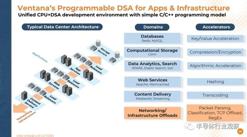
Ventana’s goal is to enable its customers to design using these DSA chiplets (whether FPGA or ASIC) to provide better workload efficiency, not just maximum SPECint throughput.
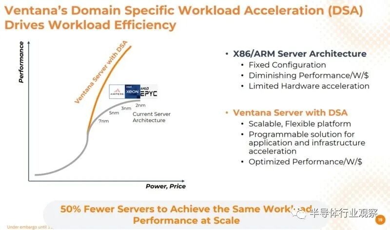
This is a good example of some DSA blocks. One really good one is infrastructure offload.
At the end of Ventana’s presentation, there was a server. This appears to be a gigabyte platform that will be a single-socket 192-core 1U server with 12-channel DDR5-5600. Don’t focus too much on the actual image, as it seems to be an Intel Skylake/Cascade Lake server with a bit of Photoshop magic around the CPU socket area.
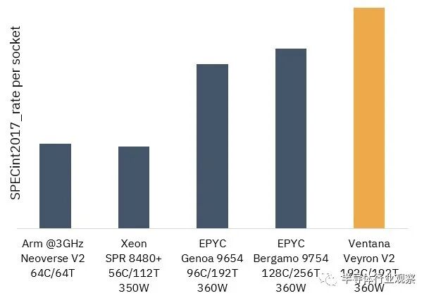
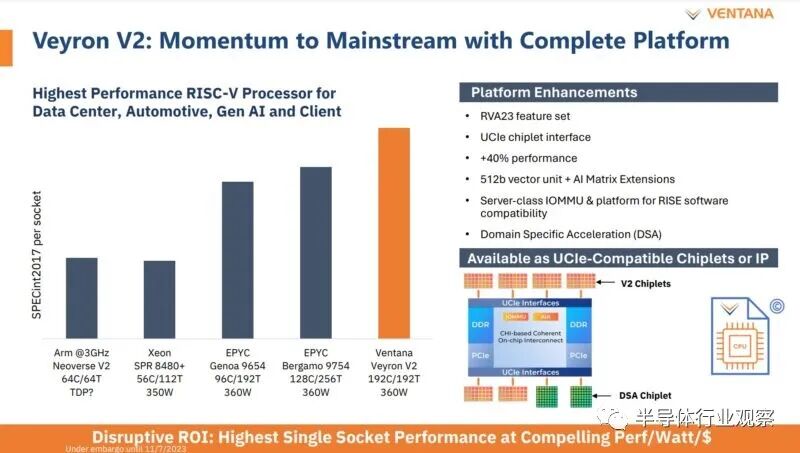
After simulating the integer performance of the Veyron V2 and the raw SPECint2017 rate per socket, we can see the following results:
If you do the math on the above chart, then at the same 360-watt power, the integer throughput of the Veyron 2 RISC-V CPU with 192 cores will be about 23% higher than AMD’s “Bergamo” Epyc 9754 processor (with 128 cores and 256 threads) at the same 360-watt thermal package, and about 34% higher performance than the 96-core “Genoa” Epyc 9654. The performance gap between the Veyron V2 chip and the 56-core “Sapphire Rapids” Xeon SP 8480+ is more like 2.7 times, which is not surprising given that it has 3.4 times the cores and 1.7 times the threads, although the V2 core must run at a lower clock speed. The declining Arm chip appears to represent AWS Graviton3, which has 64 cores and slightly higher performance than the shown Sapphire Rapids chip.
Ventana provides benchmarks for the Veyron V2 design, featuring four 128-core chiplets and eight DDR5 memory channels, with UCI-Express interconnect on the chiplets, and an I/O bug that integrates them all into the server CPU socket.
From this introduction, it seems that Ventana is indeed bringing something different. If you look at what Ampere and previously Marvell/Cavium have tried to do in the server space, you will find that they are competing directly with Intel on general-purpose computing platforms, where one major optimization is to reduce floating-point throughput on advanced TSMC process nodes to achieve better integer performance per watt. This is indeed the magic of today’s Arm servers.
Ventana is doing something different, hoping to be the CPU core of the UCIe era, expecting the market to accelerate its development. This feels a bit like the Annapurna Labs/AWS model, rather than what some well-known Arm players have been doing.
Reference Links

*Disclaimer: This article is original by the author. The content of the article reflects the author’s personal views, and Semiconductor Industry Observation reprints it only to convey a different perspective, which does not represent Semiconductor Industry Observation’s endorsement or support of this view. If there are any objections, please contact Semiconductor Industry Observation.
This is the 3578th issue shared by Semiconductor Industry Observation today, welcome to follow.
Recommended Reading
★A Prospectus, Half the History of Zhuhai Chips
★The Future of 2D Transistors
★Will Japan’s Storage Be Okay?
Semiconductor Industry Observation

『First Vertical Media in Semiconductor』
Real-time Professional Original Depth
Scan the QR code, reply to the keywords below to read more
Wafer|Integrated Circuit|Equipment|Automotive Chips|Storage|TSMC|AI|Packaging
Reply Submission to see “How to Become a Member of Semiconductor Industry Observation”
Reply Search to easily find other articles you are interested in!