Why Are Chips So Difficult to Manufacture?

Why Are Chips So Difficult to Manufacture?
In the digital age, our lives are inseparable from chips. Our computers, phones, and even the cars we travel in are equipped with numerous chips. If even one chip fails to work properly, it can affect our lives; from a malfunctioning phone to a car losing control…
While enjoying the convenience of chips, have we ever considered why chips are so important in the digital age? Why is their development and manufacturing so difficult? This story begins with the history of chips.

From Vacuum Tubes to Transistors

“In ancient times, people used knots to manage.” Since the dawn of human civilization, calculation has become an inseparable part of our lives. Whether it’s the balance of a family’s finances or the economic direction of a country, these numbers that determine the fate of families or nations all require calculation to derive. People have developed many calculation tools, such as the abacus, which uses beads to calculate, or calculators that can be pressed to get the desired results.

Why Are Chips So Difficult to Manufacture?

Copyrighted images, unauthorized reproduction may lead to copyright disputes.
As our demand for calculation continues to grow, human-based calculation methods quickly hit a bottleneck.War gave birth to the early computers: Turing developed a computer based on electric mechanical principles that cracked the German Enigma code; to crack the German Lorenz code, the British developed the “Colossus computer,” which is also considered the world’s first programmable digital computer. These machines could easily perform calculations that were difficult or even impossible for humans.
The core of the Colossus computer is the “vacuum tube,” which looks like a large light bulb filled with some metal wires. When powered, these metal wires can only have two fates:on or off, corresponding to 1 and 0 in binary.Using these two numbers, theoretically, any calculation can be performed. Our current virtual network world can also be roughly understood as being born from countless 1s and 0s.
Although the vacuum tube-based computers were powerful, they also had several limitations.On one hand, vacuum tubes were too large.The ENIAC machine manufactured by the University of Pennsylvania had over 17,000 vacuum tubes, taking up a lot of space and consuming a terrifying amount of power;on the other hand, these massive numbers of vacuum tubes also brought various risks.Statistics show that on average, this machine would experience a vacuum tube failure every two days, with each troubleshooting taking at least 15 minutes. To stably produce various 1s and 0s, people began searching for alternatives to vacuum tubes.
The famous Bell Labs made a breakthrough, and their choice was semiconductorsthese materials have conductivity based on conductors (which allow current to pass freely, like copper wires) and insulators (which do not conduct electricity at all, like glass).Under certain conditions, their conductivity can change. For example, we have all heard of “silicon” (Si), which itself is not conductive, but when combined with certain other materials, it can become conductive. The name “semiconductor” comes from this.
William Shockley of Bell Labs first proposed a theory,believing that adding an electric field near semiconductor materials could change their conductivitybut he could not experimentally prove his theory.
Inspired by this theory, his two colleagues, John Bardeen and Walter Brattain, two years later, created a semiconductor device called a “transistor.” Not wanting to be surpassed, Shockley developed a newer transistor a year later. Ten years later, the three of them received the Nobel Prize in Physics for their contributions in the field of transistors. As the transistor field continued to expand, it welcomed more new members, becoming the cornerstone of the digital age.

The Birth of Chips and Silicon Valley

As transistors gradually replaced vacuum tubes, their limitations also became apparent in practical applications.One of the main issues was how to wire thousands of transistors to form usable circuits.
To enable transistors to perform complex functions, circuits require not only transistors but also resistors, capacitors, inductors, and other components, which need to be soldered and connected. These components themselves have no standard size, making the workload for circuit production enormous and prone to errors.One solution at the time was to standardize the size and shape of each electronic component, redefining circuit design with a modular approach.
Jack Kilby of Texas Instruments was not impressed with this plan, believing it did not solve the fundamental problem—no matter how standardized, the size could not be reduced. The resulting modular circuits remained large and could not be applied to smaller devices.His solution integrated everything, placing all transistors, resistors, and capacitors on a single piece of semiconductor material, saving a lot of subsequent manufacturing time and reducing the chance of errors.
In 1958, he created a prototype using “germanium” (Ge), which contained one transistor, three resistors, and one capacitor, and when connected with wires, could generate a sine wave.This new circuit was called an “integrated circuit,” which later became commonly known as a chip.Kilby himself won the Nobel Prize in Physics in 2000 for his invention.
Why Are Chips So Difficult to Manufacture?
Copyrighted images, unauthorized reproduction may lead to copyright disputes.
Around the same time, eight engineers resigned from Shockley and started a company together, founding Fairchild Semiconductor. These eight resigners are famously known as the “Traitorous Eight” in semiconductor history. Robert Noyce was the leader among them and also thought of producing multiple components on a single piece of semiconductor material to create integrated circuits. Unlike Kilby’s method, his design integrated wires with each component into one piece. This integrated design had greater advantages in manufacturing, with the only issue being cost—Noyce’s integrated circuits, while advantageous, cost 50 times more than the original.
Just as the wars decades ago gave birth to the early forms of computers, the Cold War also brought unexpected opportunities for Noyce’s chips. As the Soviet Union launched its first artificial satellite and sent humans into space for the first time, the United States, feeling threatened, initiated a comprehensive catch-up plan. They decided to send humans to the moon as a final counterattack, but this task required immense calculations (controlling rockets, maneuvering landing modules, calculating optimal time windows, etc.), and NASA pinned its fate on Noyce’s chips:these integrated circuits are smaller and consume less power.To send humans to the moon, every gram of weight and every watt of energy had to be carefully calculated. For such extreme projects, it was undoubtedly a better choice.
In the human moon landing project, chips demonstrated their potential to the world—Noyce said that in the Apollo project’s computer, his chip operated for 19 million hours with only 2 failures, one of which was caused by external factors.
Moreover, the moon landing mission also proved that chips could operate normally in the extreme environment of outer space. After Fairchild’s rise, employees from this company branched out to establish companies like Intel and AMD, and this semiconductor-rich area later became known as Silicon Valley.

Photolithography Technology

The size of integrated circuits is much smaller than circuits composed of discrete transistor components, often requiring a microscope to see their internal structure and check quality. Jay Lathrop of Texas Instruments had a sudden idea during an observation,if a microscope can magnify things when viewed from above, could viewing from below shrink them?
This was not just for fun. At that time, the size of integrated circuits was already approaching the limits of manual manufacturing, making further breakthroughs difficult. If the designed circuit diagram could be “miniaturized” onto semiconductor materials, it might be possible to automate the manufacturing process and achieve mass production.
Lathrop quickly tested his idea.First, he bought a chemical substance called photoresist from Kodak and coated it on the semiconductor material. Then he inverted the microscope and covered the lens with a plate, leaving only a small pattern.
Finally, he let light pass through the lens and shine on the photoresist on the other end of the microscope. Under the action of light, the photoresist underwent a chemical reaction, slowly dissolving and revealing the underlying silicon material. The shape of the exposed material was identical to his original design, just reduced by hundreds or thousands of times. On the exposed grooves, manufacturers could add new materials, connect the circuits, and wash away the excess photoresist. This entire process is known as the photolithography technology for manufacturing chips.
Texas Instruments subsequently further improved this process, establishing standards for each step, which also ushered in a standardized mass production era for integrated circuits. As chips became increasingly complex, producing an integrated circuit required repeating this process at least dozens of times.
Fairchild quickly followed suit, developing its own photolithography production technology. Besides Noyce, the other seven founders of the company were also not ordinary individuals. Among them, Gordon Moore was particularly outstanding.
In 1965, he predicted the future of integrated circuits, stating that with the continuous updating of production technologies like photolithography, the number of components in chips would double every year. In the long run, the computing power of chips would grow exponentially, and costs would significantly decrease. This would lead to a clear outcome: chips would enter ordinary households in large quantities, fundamentally changing the world.This prediction by Moore later became known as “Moore’s Law,” recognized worldwide.
The premise of Moore’s Law is the continuous development and innovation of manufacturing processes. Some early companies developed nearly perfect photolithography technologies, almost like sketching lines on photoresist with light, creating circuits only one micron wide. Moreover, this technology could engrave multiple chips at once, greatly enhancing chip production capacity. However, with the increasing demand for chip manufacturing precision, micron-level photolithography machines were no longer sufficient, and nano-level photolithography machines became the new favorites.
However, developing such photolithography machines is not easy—how to perform photolithography in increasingly smaller spaces has become a bottleneck in the development of photolithography technology.

Extreme Ultraviolet Lithography Technology

By 1992, it seemed that Moore’s Law was about to fail—to maintain this law, chip circuits needed to be made smaller.Both the light source used and the lens that light passes through had new requirements.
When Lathrop initially developed photolithography technology, he used the simplest visible light. The wavelengths of these lights are around hundreds of nanometers, and the ultimate size imprinted on the chip is also in hundreds of nanometers. If smaller components (like only a few tens of nanometers) need to be imprinted on the chip, the light source must exceed the limits of visible light and enter the realm of ultraviolet light.
Some companies have developed manufacturing equipment using deep ultraviolet light (DUV), with wavelengths of less than 200 nanometers. But in the long run, extreme ultraviolet light (EUV) is the domain people aim to reach—the shorter the wavelength, the more details can be etched onto the chip.Ultimately, the target wavelength was set at 13.5 nanometers, and the Dutch company ASML became the only producer of EUV machines in the world.
The development of EUV technology took nearly 20 years. To manufacture a functional EUV machine, ASML needed to source the most advanced components globally to meet its needs. As a photolithography machine, the first requirement was the light source: to produce EUV, people needed to shoot a tin droplet with a diameter of just a few tens of microns, letting it travel through a vacuum at over 300 kilometers per hour while precisely hitting it with lasers—not once, but twice.
The first is for heating, and the second is to blast it into plasma at a temperature of 500,000 degrees, which is several times hotter than the surface of the sun.This process must be repeated 50,000 times per second to produce enough EUV. One can imagine how many advanced components such high-tech technology requires.
Why Are Chips So Difficult to Manufacture?
Copyrighted images, unauthorized reproduction may lead to copyright disputes.
Actual operations are even more complex than described above. For example, to eliminate the large amount of heat generated during laser irradiation, ventilation is needed, and the rotation speed must reach 1,000 times per second. This speed exceeds the limits of physical bearings, so magnets are needed to levitate the fan for rotation.
Moreover, the laser emitter has strict requirements for the gas density involved and must avoid reflections from the tin droplet after laser irradiation, which could affect the instrument. Just developing the machine that emits the lasers took over 10 years of research and development, with each emitter requiring more than 450,000 components.
The EUV generated by bombarding the tin droplet is hard-earned, and researchers also need to learn how to collect these rays and direct them to the chip. The wavelength of EUV is too short and is easily absorbed by surrounding materials rather than reflected. Ultimately, Carl Zeiss developed an extremely smooth mirror that could reflect EUV.
The smoothness of this mirror is beyond imagination—officially, if this mirror were enlarged to the size of Germany, the most irregular part would only be 0.1 millimeters.The company confidently believes that their mirror can guide lasers precisely to hit a golf ball located on the moon.
This complex set of equipment requires not only scientific technology but also complete supply chain management. ASML itself only produces 15% of the components for its EUV machines, with the rest coming from partners around the world. Of course, they also monitor these purchased products closely, and if necessary, they might even buy these companies to manage them directly. Such a machine is a technological product from different countries.
The first EUV machine prototype was born in 2006. In 2010, the first commercial EUV machine was delivered. In the coming years, ASML expects to launch a new generation of EUV machines, each costing $300 million.

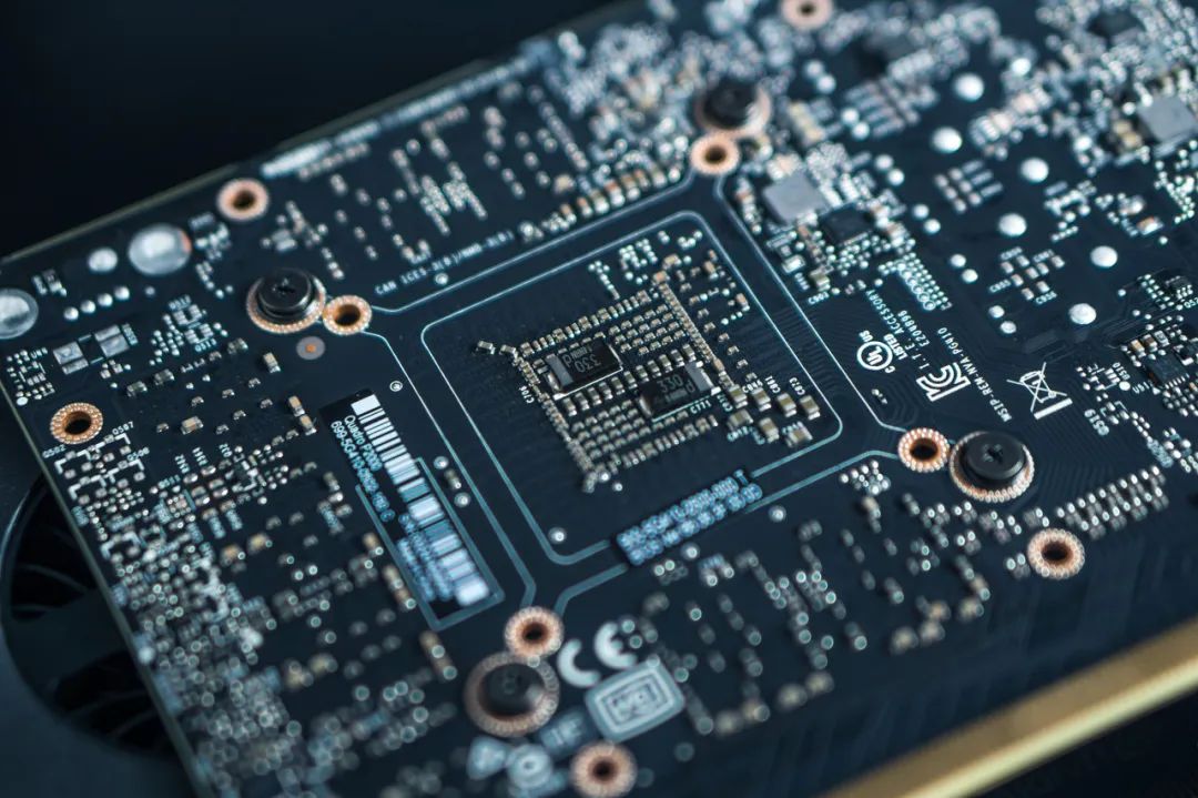
Applications of Chips

Under advanced manufacturing processes, various chips have been born.It has been summarized that in the 21st century, chips can be divided into three main categories.

The first type is logic chips, used as processors in our computers, phones, or network servers;

The second type is memory chips, classic examples include DRAM chips developed by Intel—before this product was launched, data storage relied on magnetic cores: magnetized elements represented 1, and unmagnetized elements represented 0. Intel’s approach was to combine transistors and capacitors, where charging represented 1 and not charging represented 0. Compared to magnetic cores, the new storage tool’s principle is similar, but everything is integrated into the chip, making it smaller and less error-prone. Such chips provide computers with both short-term and long-term memory during operation;

The third type of chip is called “analog chips,” which process analog signals.

Among these chips, logic chips are perhaps the most well-known.Although Intel developed the earliest DRAM memory chips, it was gradually outcompeted by Japanese companies. In 1980, Intel collaborated with IBM to manufacture central processing units (CPUs) for personal computers.
With the advent of IBM’s first personal computer, the processor built into this computer became the industry “standard,” just as Microsoft’s Windows system became the more familiar operating system for the public. This gamble also allowed Intel to completely withdraw from the DRAM field and rise again.
The development of CPUs was not achieved overnight. In fact, as early as 1971, Intel produced the first microprocessor (which, compared to a CPU, could only handle a single specific task), and the entire design process took a full six months. At that time, this microprocessor had only a few thousand components, and the design tools used were only colored pencils and rulers, which was as backward as medieval craftsmen. Lynn Conway developed a program that solved the problem of automated chip design.Using this program, students who had never designed chips could learn how to design functional chips in a short time.
By the end of the 1980s, Intel developed the 486 processor, capable of fitting 1.2 million micro-components onto a tiny silicon chip, generating various 0s and 1s. By 2010, the most advanced microprocessor chips could accommodate 1 billion transistors. The development of these chips relied on design software developed by a few oligarch companies.
Another type of logic chip—the graphics processing unit (GPU, commonly known as a graphics card)—has also gained increasing attention in recent years. In this field, Nvidia is a key player. From the outset, the company believed that 3D images were the future direction and designed a GPU capable of processing 3D graphics, along with developing corresponding software to instruct the chip on how to operate. Unlike Intel’s central processor, which “calculates sequentially,” the advantage of GPUs lies in their ability to perform a large number of simple calculations simultaneously.
No one expected that in the era of artificial intelligence, GPUs would take on a new mission. To train AI models, scientists need to continuously optimize algorithms using data, enabling models to complete tasks assigned by humans, such as recognizing cats and dogs, playing Go, or conversing with humans. At this point, GPUs, developed for “parallel processing” data to perform multiple calculations simultaneously, have a unique advantage, and they have breathed new life into the era of artificial intelligence.
Another important application of chips is in communication.Irwin Jacobs saw that chips could process complex algorithms to encode massive amounts of information, so he and friends founded Qualcomm, entering the communication field. We know that the earliest mobile phones were also called “brick phones,” resembling large black bricks.
Subsequently, communication technology developed rapidly—2G technology could transmit text and images, 3G technology could open websites, 4G was sufficient for smooth video watching, and 5G offered even greater leaps.Each “G” here represents a generation. It can be seen that each generation of wireless technology has exponentially increased the amount of information transmitted via radio waves. Nowadays, we feel impatient with even slight delays while watching videos on our phones, unaware that over a decade ago, we could only send text messages.

Why Are Chips So Difficult to Manufacture?

Copyrighted images, unauthorized reproduction may lead to copyright disputes.
Qualcomm participated in the development of mobile technologies from 2G onwards. Utilizing chips that evolve according to Moore’s Law, Qualcomm can place more phone calls into the vast space through infinite spectrums. To upgrade to 5G networks, not only do new chips need to be installed in phones, but new hardware must also be installed in base stations. These hardware and chips, with their powerful computing capabilities, can transmit data faster wirelessly.

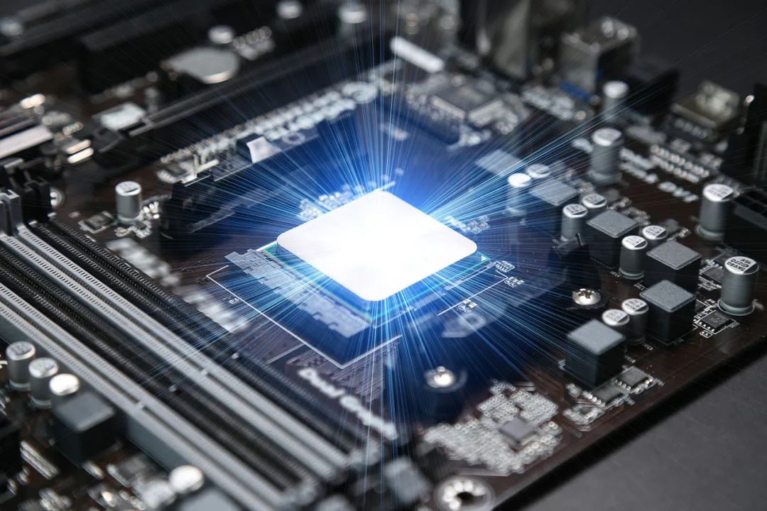
Manufacturing and Supply Chain

In 1976, almost every chip design company had its own manufacturing base. However, separating chip design from chip manufacturing and outsourcing manufacturing to specialized foundries could significantly reduce costs for chip design companies.
Taiwan Semiconductor Manufacturing Company (TSMC) was born, promising to manufacture chips without designing them. This way, chip design companies do not have to worry about leaks of confidential information. TSMC also does not rely on selling more chips—its success is tied to its customers’ success.
Before TSMC, some American chip companies had already set their sights on the vast Pacific Ocean: in the 1960s, Fairchild established a center in Hong Kong to assemble various chips shipped from California. In its first year of production, the Hong Kong factory assembled 120 million devices, with low labor costs but high quality. Within a decade, nearly all American chip companies had set up assembly plants in Asia. This laid the foundation for the current supply chain pattern centered on East Asia and Southeast Asia.
Asia’s efficiency and obsession with quality quickly impacted America’s position in the chip industry. In the 1980s, executives from companies responsible for chip quality testing unexpectedly discovered that the quality of chips produced in Japan had surpassed that of the United States—the failure rate of ordinary American chips was 4.5 times that of Japanese chips, and the worst American chips had a failure rate 10 times that of Japanese chips!“Made in Japan” was no longer synonymous with cheap but low-quality products. More frighteningly, even the most squeezed American production lines were not as efficient as Japan’s. “Japan’s capital cost was only 6% to 7%, while at my best, it was still 18%,” said AMD’s CEO Jerry Sanders once.
The financial environment also played a role:At that time, the United States raised interest rates to curb inflation, with rates soaring to 21.5%; while Japanese chip companies were supported by financial groups, and the public was accustomed to saving, allowing banks to provide large amounts of low-interest loans to chip companies. With capital support, Japanese companies could aggressively seize the market.
In this back-and-forth, companies capable of producing advanced logic chips concentrated in East Asia, and the chips produced were subsequently sent to nearby locations for assembly. For example, Apple’s chips are primarily produced in South Korea and Taiwan, then sent to Foxconn for assembly.These chips include not only the main processors but also chips for wireless networks and Bluetooth, camera chips, motion sensing chips, etc.
As the ability to manufacture chips gradually concentrated in a few companies, these originally foundry companies gained greater power, such as coordinating the needs of different companies and even setting rules. Since the companies responsible for designing chips currently lack the ability to manufacture them, they can only follow suggestions. This growing power has also become one of the topics in current geopolitical struggles.

Conclusion

From the machines that decrypted WWII codes to the spacecraft that sent humans to the moon. From portable music players to airplanes and cars used in daily travel, to the phones and computers we use to read this text, all these devices rely on chips.
Every day, an ordinary person’s life uses dozens to hundreds of chips.All of this is inseparable from the development of chip technology and the production and manufacturing of chips.Chips are one of the most important inventions of this era. Developing new chips not only requires scientific and technological support but also advanced manufacturing capabilities and a civilian market that applies these chips.
The layout of chip design and manufacturing capabilities has undergone decades of changes, forming the current pattern and generating unique significance in this era.This article hopes to provide interested readers with references by tracing some important industrial nodes regarding chips over the past few decades.

Planning and Production

Author: Ye Shi, popular science creator

Reviewed by: Huang Yongguang, associate researcher at the Institute of Semiconductors, Chinese Academy of Sciences

Planning: Xu Lai

Editor: Yi Nuo

Previous Issues

Selected

Why Are Contemporary Women Trapped in “Perfectionism” and Why Is It So Hard to Overcome?

Women’s Disease Rate is 8 Times That of Men! Pay Attention to These 5 Dietary Points!

Beware! Smart Bracelets Become “Digital Handcuffs,” Many People Are Forced to Do This…

Why Are Chips So Difficult to Manufacture?

Light Up “Watch”

Let’s Learn Together!

Why Are Chips So Difficult to Manufacture?

Leave a Comment