Abstract:Embedded hardware design is a systematic task. For engineers, understanding the processes and general methods involved is significant for carrying out their work. Today, we will briefly discuss the general processes in hardware design.
1. Requirement Analysis
Requirement Analysis involves collaborating with clients to analyze requirements and determine the final needs, establishing guiding documents such as product technical plans and system block diagrams. Two key points to pay attention to are:
First, the product design should reflect the true needs of users and possess a certain market foresight, ensuring that products in the same series have inheritability and scalability, while considering partial compatibility with other product series.Second, the quality of the product technical plan is crucial to the success or failure of a product. Spending more time on the product technical plan in the early stages can save more time later on resolving product bugs, such as choosing communication methods, whether to use CAN or RS-485, etc.
2. Hardware Schematic Design
Hardware Schematic Design involves selecting key components and communicating with suppliers. The circuit design should consider derating, outputting schematic design documents, reviewing schematic outputs, and producing hardware-software interface documents.
Key components refer to the selection of MCUs and primary/secondary power supplies, whether to use domestic or foreign brands, whether they are stable mass production products, whether delivery times meet requirements, whether they are common materials, and whether there are other pin-to-pin alternatives available in the market. The schematic review needs to go through the circuit one by one, focusing on new circuit parts, and performing preliminary simulations. If conditions allow, build the circuit for verification.The hardware-software interface document can generally be output to the driver engineer after the schematic is finalized, as the driver engineer can work on related tasks during the PCB layout, prototyping, and assembly phases without delaying the project timeline, allowing the driver to complete basic work once the prototype returns.
3. PCB Design and System Stacking
PCB Design and System Stacking occurs after the schematic is finalized. We will output to the PCB layout engineer for pre-layout. This process generally requires repeated iterations, constant compromises, and optimizations to achieve a reasonable layout. After the pre-layout is completed, a 3D model is output to the structural engineer to check for interferences, and adjustments are made to finalize the system stacking plan. Key points to note in PCB design include:
First, focus on layout; a well-organized layout makes subsequent work easier. The PCB layout engineer needs to have a deep understanding of the circuit.Second, power layout routing; many product issues stem from power problems, so it is crucial to pay attention to the schematic design and PCB layout routing, considering safety regulations and necessary certifications.Third, handling of key signals, including clock, high-speed, differential, analog, reset, and other sensitive signals, ensuring proper isolation between signals.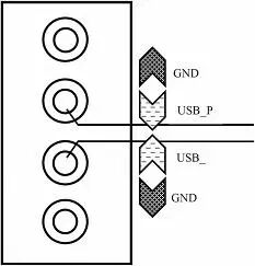
4. Prototype Production
Prototype Production involves producing the prototype after the PCB is completed, which generally requires hardware engineers to follow up, including outputting the BOM, organizing the assembly files (by the PCB engineer), communicating issues during the factory assembly process, and confirming the first piece.
5. Prototype Debugging
Prototype Debugging typically involves the following steps:
First, after the prototype returns, conduct a visual inspection of the PCBA for issues such as poor soldering, solder shorts, reversed polarity components, missed soldering, and obvious soldering errors.Second, before powering on, use a multimeter to check for short circuits in the power output, generally checking for shorts to ground for each power supply.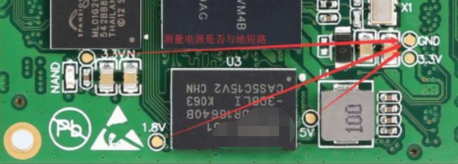 Third, measure the system voltages with a multimeter to ensure they are within the designed range, such as system 5V, system 3.3V, system 2.8V, system 1.2V, and then use an oscilloscope to test the power on/off to ensure there are no significant steps, ringing, or overshoot issues.Fourth, test the crystal oscillator to check if the system crystal oscillates upon power-up, such as 24MHz or 32.768KHz.Fifth, test the reset circuit; if there is a hardware watchdog circuit, test the WDG_WDI and RESET signal waveforms and device operating status under feeding conditions, and check if the WDG_WDI and RESET signals meet the timing specifications in the datasheet when feeding is stopped.Sixth, perform a power-on test (to check if the system operates normally, which can also be done via serial output of its operating status).
 Seventh, specific hardware debugging items will depend on the project, as many other issues may arise during hardware debugging, such as abnormal power on/off, 4G ping network issues, screen artifacts, speaker distortion, and SD card communication anomalies.
6. Prototype Debugging
Prototype Debugging typically involves the following two steps:
First, after the prototype returns, conduct a visual inspection of the PCBA for issues such as poor soldering, solder shorts, reversed polarity components, missed soldering, and obvious soldering errors.Second, before powering on, use a multimeter to check for short circuits in the power output, generally checking for shorts to ground for each power supply.ENDAuthor: BrainSource: 8th Line EngineerCopyright belongs to the original author. If there is any infringement, please contact for removal.▍Recommended Reading3 Git Visualization ToolsEye-catching Linux Terminal Tools!Why are Chinese numbers grouped by four digits while Western numbers are grouped by three?→ Follow for more updates ←