Welcome FPGA engineers to join the official WeChat technical group.
Clickthe blue textto follow us on FPGA Home – the best and largest pure FPGA engineer community in China

Reference: http://www.zynqbook.com/
ZYNQ Architecture
-
Dual-core ARM Cortex-A9 Processor: The ARM Cortex-A9 is an application-level processor capable of running a complete operating system like Linux.
-
Traditional Field Programmable Gate Array (FPGA) Logic Components: Based on the Xilinx 7 series FPGA architecture.
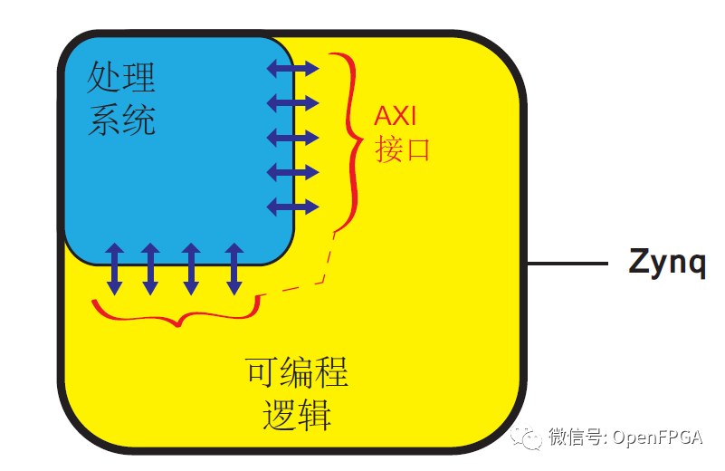
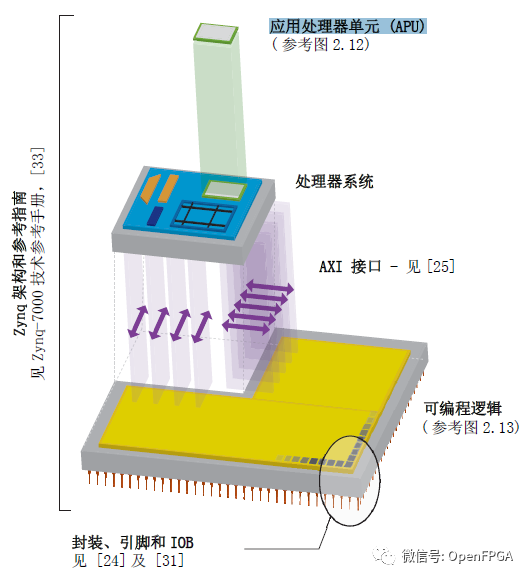
This architecture implements the industrial standard AXI interface, achieving high bandwidth and low latency connections between the two parts of the chip.
This means that both the processor and logic parts can perform at their best without the interface overhead that would occur between two discrete chips.
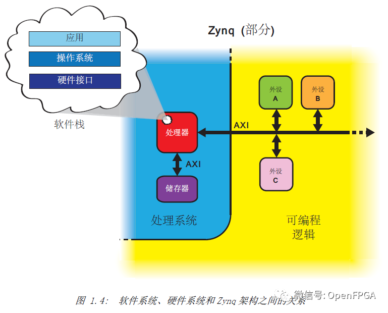
Peripherals are functional components outside the processor, typically serving one of three functions: (1) Co-processors — units that assist the main processor, often optimized for specific tasks; (2) Cores that interact with external interfaces, such as connections to LEDs and switches, codecs, etc.; (3) Additional memory units.
PS has a fixed architecture that houses the processor and system memory area.
While PL is completely flexible, providing designers with a “blank canvas” to create custom peripherals or reuse standard peripherals.
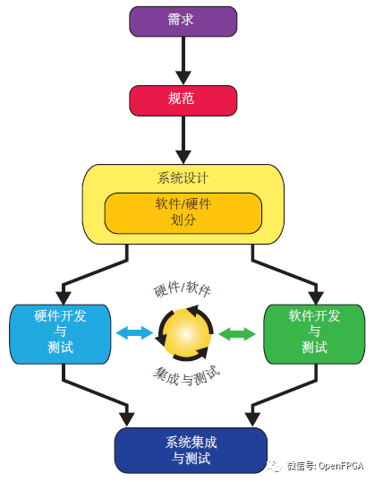
Basic Model of ZYNQ SoC Design Flow
ZYNQ Chip
Processor System (PS)
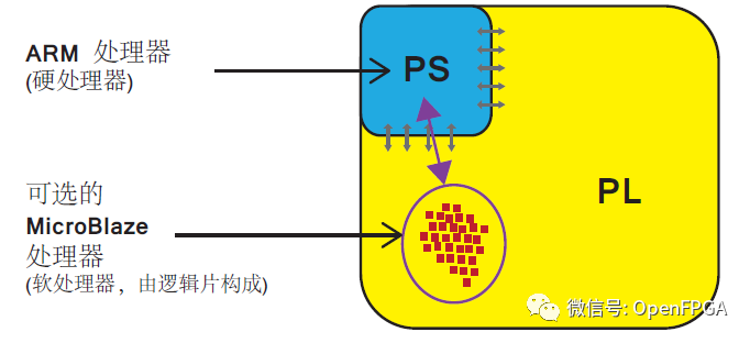
ARM is a “hard” processor; another option outside of hardware processors is a “soft” processor like Xilinx’s MicroBlaze, which is composed of units from the programmable logic part. This means that the implementation and deployment of a soft processor is equivalent to any other IP block in the FPGA logic structure. Tasks that do not require high performance can be offloaded from the main ARM Cortex-A9 processor to the soft processor, allowing the soft processor to work alongside ARM to enhance overall performance.
In the PS, there is not only the ARM processor but also a set of related processing resources that form an Application Processing Unit (APU), along with extended peripheral interfaces, cache memory, memory interfaces, interconnect interfaces, and clock generation circuits.
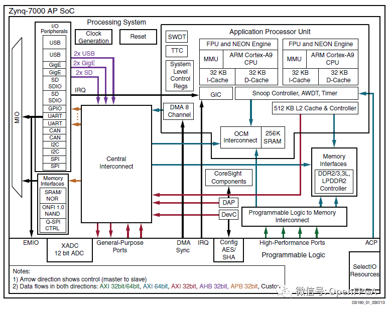
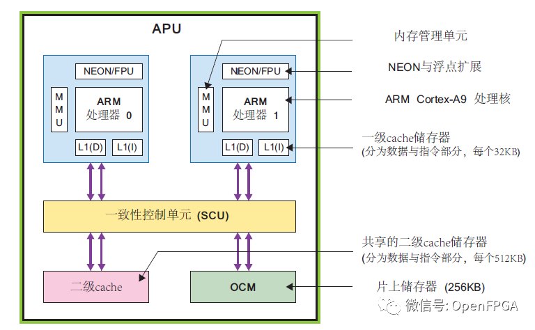
Communication between the processor system and external interfaces is primarily achieved through Multiplexed Input/Output (MIO). Such connections can also be established through Extended MIO (EMIO), which does not provide a direct path between the PS and external connections but utilizes shared I/O resources from the PL.
Available I/O includes standard communication interfaces (SPI, I2C, USB, SD, CAN, UART, GigE) and General Purpose Input/Output (GPIO).
Programmable Logic (PL)
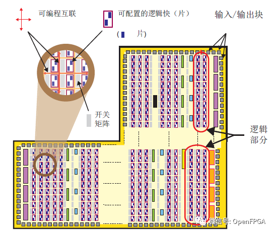
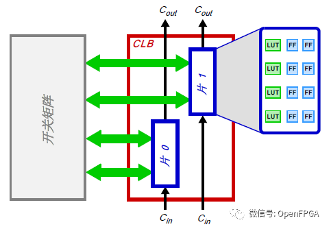
LUT – Lookup Table (https://www.cnblogs.com/lbf-19940424/p/6564885.html)
FF – Flip-Flop, a sequential circuit that implements a 1-bit register with a reset function. One use of FF is to implement latches.
CLB – Configurable Logic Block
IOB – Input/Output Block (IOB) – implements the interfacing between PL logic resources and provides physical device “pads” to connect to external circuits. Each IOB can handle a single bit of input or output signal. IOBs are typically located around the perimeter of the chip.
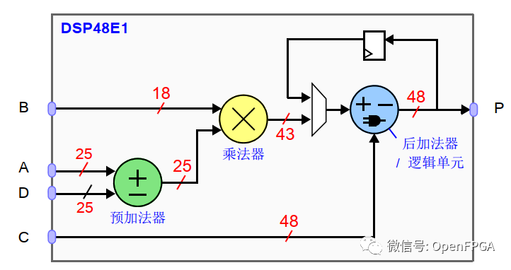
In addition to the general parts, there are two special-purpose components: block RAM to meet dense storage needs and DSP48E1 chips for high-speed arithmetic.
General-purpose IOBs
Communication interfaces — including PCI Express, Serial RapidIO, SCSI, and SATA
Other programmable logic expansion interfaces — XADC, clock, programming, and debugging
Interface between Processor System and Programmable Logic
1. AXI Standard — Advanced eXtensible Interface
There are three types of AXI4 bus protocols.
• AXI4 [2] — for memory-mapped links, supporting the highest performance: data transfers of up to 256 data words (or “data beats”) per given address. • AXI4-Lite [2] — a simplified link that supports transferring one data item (non-burst) per connection. AXI4-Lite is also memory-mapped: this protocol transfers one address and a single data item at a time.
• AXI4-Stream [1] — for high-speed streaming data, supporting bulk transfers of unlimited data sizes. There is no addressing mechanism; this bus type is best suited for direct data flow between source and destination (non-memory mapped).
Interconnect — the interconnect is essentially a switch that manages and directly passes communication between connected AXI interfaces. There are several interconnects within the PS, some of which are directly connected to the PL (as shown in Figure 2.9), while others are for internal connections only. Connections between these interconnects are also formed using AXI interfaces. Interface — point-to-point connections for transmitting data, addresses, and handshake signals between hosts and slaves within the system. (M – Master, S – Slave)
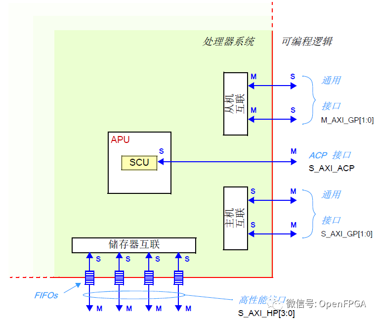
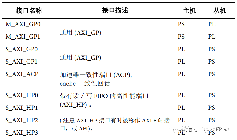
• General Purpose AXI — a 32-bit data bus suitable for medium to low-speed communication between PL and PS. The interface is a transparent pass-through without buffering. There are four general interfaces in total: two PS as masters and two PL as masters. • Accelerator Coherency Port — a single asynchronous connection between the SCU (System Coherency Unit) within the PL and APU, with a bus width of 64 bits. This port is used to achieve cache coherence between APU and PL units. PL acts as the master. • High Performance Ports — four high-performance AXI interfaces with FIFO buffering to provide “bulk” read and write operations, supporting high-rate communication between memory units in PL and PS. Data widths are 32 or 64 bits, with PL as the master in all four interfaces.
2. EMIO Interface
3. Other PL-PS Signals
Other signals crossing the PS-PL boundary include watchdog timer, reset signals, interrupts, and DMA interface signals.
Security
Summary
In conclusion:
I believe that in addition to the innovation of the overall architecture, the flexible I/O is also a part of why ZYNQ has become popular:
Multiplexed I/O (MIO): What is the concept of peripheral I/O multiplexing on the PS side? As mentioned earlier, ZYNQ is primarily divided into two major modules: PS/PL. The peripherals on the PS side, such as USB/CAN/GPIO/UART, all require pins to interact with the outside world. This multiplexing concept is similar to pin multiplexing in common microcontrollers and processors. However (this is important), ZYNQ supports up to 54 PS pins for MIO, which provides very high flexibility for configuration, greatly facilitating hardware design and PCB layout! The MIO configuration can be achieved flexibly using Vivado software, as shown in the figure below.
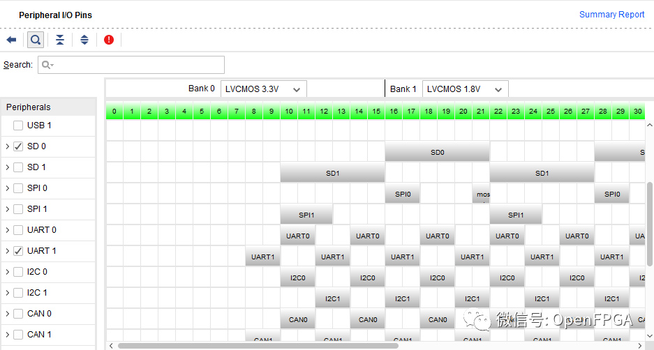
Hardware engineers often find it challenging to layout and route a complex system, and often fall into deep EMC pitfalls due to unreasonable layout and routing. The high flexibility of ZYNQ’s I/O pins undoubtedly provides great convenience in circuit design, allowing for very flexible PCB layout and routing, thus greatly improving EMC performance.
Flexible PS-PL Interconnection Interface
-
Extended Multiplexed I/O (EMIO): If you want to access PL through PS without wasting the AXI bus, you can use the EMIO interface to access PL. Among the 54 I/O, some can only be used for MIO, most can be used for either MIO or EMIO, and a few pins can only be accessed through EMIO.
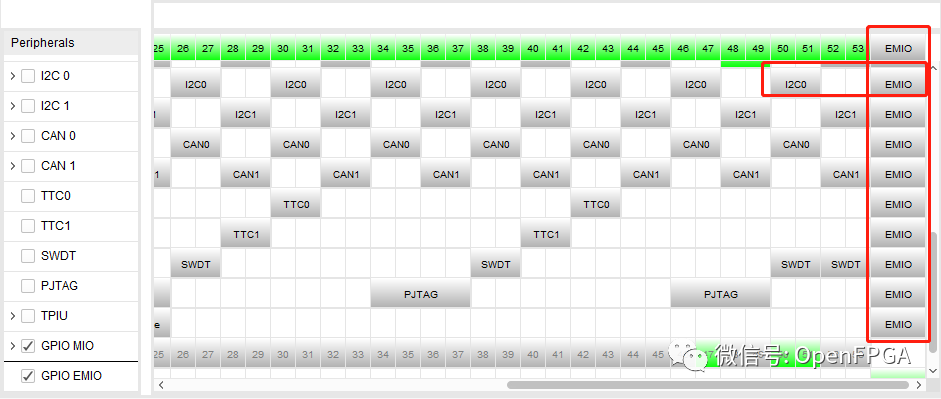
As shown in the figure above, for example, I2C0 can be mapped to the PL side pin output through EMIO, which undoubtedly adds more flexibility!
-
PS-PL Interface HP0-HP3: As shown in the architecture diagram, AXI high-performance slave ports (HP0-HP3) implement the PS-PL interface.
-
Configurable 32-bit or 64-bit data width. -
Can only access on-chip memory OCM (On-chip Memory) and DDR. -
AXI FIFO interface (AFI) uses 1KB FIFOs to buffer large data transfers. -
PS-PL Interface GP0-GP1: As shown in the architecture diagram, AXI general-purpose ports.
-
Two PS master interfaces connect to two PL slave devices. -
32-bit data width. -
A 64-bit Accelerator Coherency Port (ACP) AXI slave interface connected to CPU memory, which is an asynchronous cache coherence access point from PL to PS. The ACP can be accessed by many PL masters in the same way as the APU processor accesses the memory subsystem. This can improve overall performance, reduce power consumption, and simplify software. The performance of the ACP interface is the same as that of a standard AXI slave interface, supporting most standard read and write operations without requiring additional coherence operations in PL components.
-
DMA, interrupts, event signals:
-
Processor event bus signals to the CPU. -
PL peripheral IP interrupts to the PS general interrupt controller (GIC). -
Four DMA channel RDY/ACK signals. -
Extended Multiplexed I/O (EMIO) allows PS peripheral ports to access PL logic and device I/O pins.
-
Clock and reset signals:
-
Four PS clock enable controls connected to PL. -
Four PS reset signals connected to PL.

Welcome FPGA, embedded, signal processing engineers to follow our public account.

National Largest FPGA WeChat Technical Group
Welcome everyone to join the national FPGA WeChat technical group, which has tens of thousands of engineers, a group of technology-loving engineers. Here, FPGA engineers help each other, share knowledge, and the technical atmosphere is strong! Hurry up and invite your friends to join!!

Press and hold to join the national FPGA technical group.
FPGA Home Component City
Advantage component services, please scan the code to contact the group owner: Jin Juan Email: [email protected] Welcome to recommend to procurement
ACTEL, AD part advantage ordering (operating the full series):
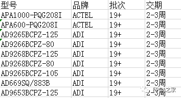
XILINX, ALTERA advantage stock or ordering (operating the full series):
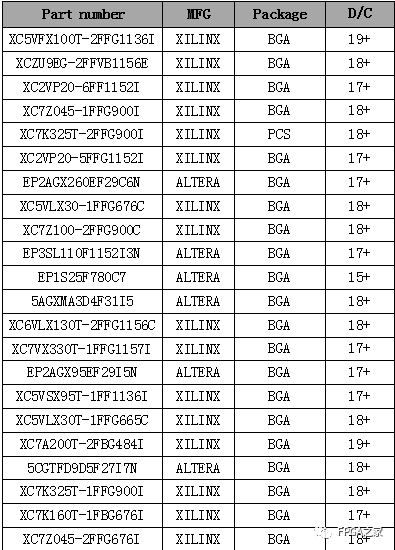
(The above components are partial models; for more models, please consult group owner Jin Juan.)
Service philosophy: FPGA Home Component City aims to facilitate engineers in quickly and conveniently purchasing components. After years of dedicated service, our customer service covers large domestic listed companies, military research units, and small and medium enterprises. Our biggest advantage is emphasizing service above all, and ensuring fast delivery and competitive prices!
Directly operated brands: Xilinx, ALTERA, ADI, TI, NXP, ST, E2V, Micron, and over a hundred other component brands, especially good at handling embargoed components from Europe and the US. We welcome engineering friends to recommend us to procurement or consult us directly! We will continue to provide the best service in the industry!

Official brands thanks from FPGA technology group: Xilinx, Intel (Altera), Microsemi (Actel), Lattice, Vantis, Quicklogic, Lucent, etc.