SDF files replace the delay information specified in STD/IO/Macro gate-level Verilog with the actual physical delay information extracted from QRC/Star-RC during VCS/NC-Verilog post-simulation runtime. Therefore, if the condition information in the SDF file is not present in the Verilog specify, it will raise a warning of SDFCOM_INF, meaning IO PATH not found.
This article analyzes the Header Section information of SDF and focuses on explaining the Cell Entries, especially the Delay Entries.
-
The following text will first discuss the first part of the SDF file, the Header Section.

-
SDF Version Entry, including 1.0, 2.1, 3.0, SDF 3.0 was released in 1995.
-
Design Name Entry, the top-level design name.
-
Date Entry, the SDF generation date, produced by PT or Tempus.
-
Vendor Entry, vendor information, as shown below.

-
Program Version Entry.
-
Hierarchy Divider Entry.
-
Voltage Entry, the official explanation of SDF 3.0 is as follows.

-
Process Entry, the official explanation of SDF 3.0 is as follows.

-
Temperature Entry, the official explanation of SDF 3.0 is as follows.


-
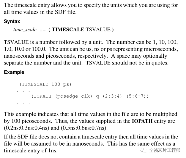
Timescale Entry, the official explanation of SDF 3.0 is as follows.
-
The following text continues to explain the second part of the SDF file, Cell Entries:

-
PATHPULSE
-
PATHPULSEPERCENT
-
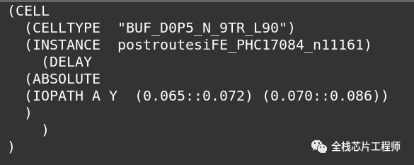
ABSOLUTE Delays
-
INCREMENT Delays

-
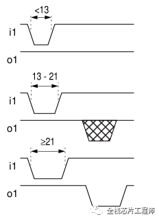
When the low-level pulse output from i1 to o1 is less than 13ns, the lowlevel pulse is ignored directly; -
When the low-level pulse output from i1too1 is between 13ns~21ns, the output is X state; -
When the low-level pulse output from i1too1 is greater than 21ns, the normal low-level output;

4. INCREMENT Delays
Used to add to the delay data in the Verilog specify, INCREMENT Delays can have negative values, if the added delay is negative, some EDA tools may not support it or force the delay to be 0.

Chip Full Process Training
Chip Training is about to start, quickly surpass your peers! Sign up contact WeChat: 13541390811
-
Jingxin SoC front-end, middle-end, and back-end low power full process practical training(Price is less than 1/6 of the industry)
-
Jingxin SoC front-end video + documents + practical + one-to-one lifetime tutoring practical training
-
Jingxin SoC middle-end video + documents + practical + one-to-one lifetime tutoringpractical training
-
Jingxin SoC back-end video + documents + practical + one-to-one lifetime tutoringpractical training
-
12nm 2.5GHz A72 low power DVFS practical training(Price is less than 1/3 of the industry)
-
12nm 2.5GHz A72 DFT practical training(Price is less than 1/3 of the industry)
-
RISC-V MCU 40nm full chip PR practical training
-
DDR4/3 project practical training
-
MIPI CSI2 + ISP image processing + HDMI practical training (i.e. Jingxin SoC front-end)
-
MIPI CSI2 + ISP image processing + H.265 + USB + MAC practical training (in development)
-
Advanced Codec H.265/H.264 practical training (in development)
Introduction to Chip Design Service:
-
Provide SoC, MCU, ISP, CIS and other chip design, verification, DFT design services
-
Provide DDR/PCIE/MIPI/CAN/USB/ETH/QSPI/UART/I2C and other IP design
-
Provide backend design for 7nm, 12nm, 28nm, 40nm, 55nm, 65nm, 90nm, etc.
-
Provide customized chip design services for universities and enterprises, design training services
In addition, the editor shares knowledge about chip design, verification, DFT, and backend full process knowledge and a large number of technical documents in the knowledge community. Everyone is welcome to join the discussion and learning, and make progress together!

【Let every student be able to design a SoC/MCU chip】
【The only one on the internet】Jingxin SoC is a low-power ISP image processing SoC used for 【chip full-process design training】, using a low-power RISC-V processor, built-in ITCM SRAM, DTCM SRAM, integrated with MIPI, ISP, USB, QSPI, UART, I2C, GPIO, Ethernet MAC controller, etc. IP, designed with SMIC40 process.

-
High-speed interface Verilog design implementation -
From image algorithm to RTL design implementation -
MIPI, ISP’s Verilog implementation and simulation -
Lint, CDC checks and UVM verification -
Post-simulation
Just the content of the front-end course is equivalent to 5-6 courses from other training institutions.
-
DFT design (chip-level) -
Synthesis logic synthesis (chip-level) -
Low power UPF design, CLP technology -
formal verification and other technologies
(3) In the SoC back-end course, you will learn
-
Low power design
-
Layout routing (low power FF flow) -
StarRC/QRC -
STA/Tempus -
Power analysis -
DRC/LVS design
Just the content of the back-end course is equivalent to 3-4 courses from other training institutions.

Join the knowledge community and become part of the chip design knowledge treasure!
Knowledge community of SoC training camp

Today’s introduction ends here, and then the SoC course provides a server for everyone to practice! Take you from algorithms, front-end, DFT to back-end full process participation in SoC project design.
Please contact the number owner to sign up! Contact WeChat: 135-4139-0811
The data path of Jingxin SoC training camp for image processing:
The CRG design of Jingxin SoC:

One-click completion of C code compilation, simulation, synthesis, DFT insertion, formal verification, layout routing, parasitic parameter extraction, STA analysis, DRC/LVS, post-simulation, formal verification, power analysis, and other full processes. The upgraded chip design project V2.0 flow is as follows:
SoC one-click execution flow

MIPI DPHY+CSI2 Decoding

Classic design in digital circuits: implementation of multiple communication data Lane Merging design.
Classic design in digital circuits: implementation of multiple communication data Lane Distribution.

UPF Low Power Design
Full chip UPF low power design (including DFT design)

The power consumption before low power design is 27.9mW.


Voltage drop check:

Low power check:

Chip layout design V1.0

Chip layout design V2.0

The DRC/LVS of low power design, the LVS practice of the chip top layer has extremely high practical value and is challenging! Unique experience sharing in the industry.

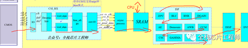
ISP Image Processing
-
dpc – Bad point correction

-
blc – Black level correction

-
bnr – Bayer noise reduction
-
dgain – Digital gain
-

-
demosaic – Demosaicing

-
wb – White balance gain
-
ccm – Color correction matrix
-
csc – Color space conversion (integer optimized RGB2YUV conversion formula)
-
gamma – Gamma correction (brightness based on table-based Gamma correction)
-
ee – Edge enhancement

-
stat_ae – Auto exposure statistics
-
stat_awb – Auto white balance statistics
CNN Image Recognition

Supports handwritten digit AI recognition:

Simulation results: simulated recognition of the numbers 7, 2, 1, 0, 4, 1, 4, 9

Jingxin Micro SoC Team Business
Introduction to the Jingxin Micro SoC team business:
-
Provide the most complete process actual chip project training on the internet
-
Provide SoC, MCU, ISP, CIS and other chip design services
-
Provide chip design, verification, DFT design services
-
Provide backend design services, processes include 7nm, 12nm, 28nm, 40nm, 55nm, 65nm, 90nm, 110nm, 180nm, etc., provide wafer production channels
-
Provide customized chip design training and employment recommendation and guidance for universities and enterprises
Rich tutorial documents


Students in the 7-day sprint PR training camp ask how to add PAD to IO? Please think about how Jingxin SoC’s IO and PAD achieve the best?

Join the knowledge community and become part of the chip design knowledge treasure!
Knowledge community of SoC training camp

SoC training camp VIP students ask why the low power cell is not inserted into the netlist?
Although asking questions is encouraged, when we encounter problems, we should first think proactively and solve problems actively. If we really can’t solve them, we can ask for help. This way, we will grow faster.
First, the editor got this question and opened the log. Checking the log is a virtue in IC design! I found that after the EDA tool ingested the UPF file, it raised the following warning, using many ff libraries.

The above error shows that the UPF specified voltage is 0.99V, while the CELL is 1.20V. The voltage mismatch caused the netlist generated by logic synthesis to not insert the MV CELL. Note that during synthesis, we used the ss library; how could it be the ff library? Opening the constraint script revealed the following bug:

So, change the constraint to replace ff with ss. Run it again, and the results will come out:

In the low power design part, I will leave a small bug inside the design. It is very simple, and I will not disclose the answer. Everyone must think more and practice more; this way, you will learn more deeply.
Training students please note that Jingxin SoC uses the always-on power domain voltage domain pwrdown_mux signal as the switch control signal for the power switch cell. However, there is a small issue in the design, which is not exactly a bug, but for the UPF low power flow, it is undoubtedly a bug!
Training students please log in to the server to track the pwrdown signal and pay attention to its load situation. The RTL code is as follows:

Combining the netlist output from PR, we will conduct a clp low power check. The script can be found on the server. It can be found that the clp reports that the switch control signal for the power switch cannot be found.

It must be said that clp checking is so important for low power and for chip design! The value of Jingxin SoC lies in connecting all these small knowledge points of the chip design full process! What are you hesitating about? Hurry up and sign up!
During the mid-process of chip design, Jingxin SoC will insert isolation and other cells in the UPF constraint, but cannot insert power switch and other cells. Therefore, the control signal pwrdown_mux for the power switch cell, in the absence of load, will be optimized away. Therefore, it is necessary to set the above MUX device to dont_touch or make pwrdown_mux a module port and prohibit auto_ungroup (and set no_boundary_optimization), so that this signal can be reserved for the back-end to implement power switch control. Please complete the code modification and complete the following tasks based on the full set flow environment:
-
Lint check, front-end simulation,
-
Complete mid-end and back-end flow,
-
Complete clp check, complete post-simulation
Students in the 7-day sprint PR training camp ask why the same floorplan runs quickly for some students while others encounter numerous DRC issues (EDA tools keep iterating) causing the tools to never finish running. What specific issues are there?
First, the editor found that the student defined TM2 as horizontal, while students familiar with Jingxin’s process know that the preference direction of TM2 is VERTICAL.

Checking Jingxin’s lef library file can also confirm:

What is the impact of using the wrong direction? Everyone should practice on Jingxin SoC’s back-end flow to find out the truth.
Students in the 7-day sprint PR training camp ask why PR, which took a day and night (24 hours) to complete routing, still has many DRC errors? The editor has minimized the design scale to speed up PR design. In fact, it can be completed in 2 hours. Why is it so slow? The reason is the routing of low power cells. Specific reasons and solutions are welcome to join the Jingxin training camp for discussion.

Its errors are mainly concentrated on M4. Please think about how to solve it.

Students in the 7-day sprint PR training camp ask why the second PG pin (VDDG) of the power switch cell is connected from M1 and not M2. Please think about what problems this may cause and how to solve it.

Students in the 7-day sprint PR training camp ask how to handle Corner Pad LVS that does not pass?

After completing the front-end design simulation and DFT of the Jingxin SoC training, we come to the back-end flow. This tutorial teaches you how to run the digital back-end flow with one click.

The script command for generation is as follows:
tclsh ./SCRIPTS/gen_flow.tcl -m flat all

Before generating the flow script, it is necessary to configure setup.tcl and other related parameters. Please refer to the 【the only one on the internet】【full-stack chip engineer】 for self-developed Jingxin SoC front-end engineering, DFT engineering, back-end engineering, taking you from algorithms, front-end, DFT to back-end full process participation in SoC project design.
Students in the Jingxin SoC training camp ask why Innovus reports an error when reading the completed floorplan def file? First, check the log:

Reading floorplan file – ./data_in/DIGITAL_TOP.def (mem = 1595.0M).
#% Begin Load floorplan data … (date=10/23 22:38:01, mem=1579.3M)
**ERROR: (IMPFP-710): File version unknown is too old.
In the past EDI period, we could load the floorplan by defining fp_file:
set vars(fp_file) “./data_in/DIGITAL_TOP.def”
However, now Innovus has upgraded and abandoned the loading method of fp_file. Of course, we can use the old version of EDI9.1 and earlier to add fp_file and then save it as a new version, but this method is obviously unnecessary. Just as the log indicates, checking the log is a very good engineer’s habit.
The input floorplan file is too old and is not supported in EDI 10.1 and newer.
You can use EDI 9.1 and before to read it in, then save again to create a new version.
The editor’s intuition tells me to check which def version the student saved?

How to solve this? Please everyone join the Jingxin training camp for practice.
Jingxin SoC uses many asynchronous FIFOs. Students interested in the implementation of asynchronous RTL can extract the asynchronous FIFO and check the layout connection:

Check the area of all asynchronous FIFO cells;
dbget [dbget top.insts.pstatus unplaced -p].area
Check the names of all asynchronous FIFO cells:
dbget [dbget top.insts.pstatus unplaced -p].name
So how can we extract the asynchronous path to observe the layout routing? How to let report_timing? More content can be found in the knowledge community and SoC training camp.
Front-end Design Directory

Middle-end Design Directory

Back-end Design Directory

Welcome to join the 【Full-Stack Chip Engineer】 knowledge community to exchange technology, and communicate about the full process design from algorithms, front-end, DFT to back-end.Click the image below to join the knowledge community!

Welcome to join the SoC MCU full process design exchange group, first add my WeChat, verify the position, and then enter the group!
SoC MCU full process design exchange group 4
SoC MCU full process design exchange group 3
SoC MCU full process design exchange group 2
SoC MCU full process design exchange group 1
Welcome to join the CMOS image sensor + ISP exchange group, first add my WeChat, verify the position, and then enter the group!
CMOS image sensor + ISP exchange group 2
CMOS image sensor + ISP exchange group 1
