Technical Support: 199-6293-0018
In the modern electronics manufacturing field, Printed Circuit Boards (PCB) are the core for connecting electronic components, achieving electrical connections and signal transmission. However, the issue of PCB warping has always been a challenge in the manufacturing process, as it not only affects the physical integrity of the product but may also lead to performance degradation and reliability problems.The Meinuo Photonics 3D Confocal Microscope can not only provide ultra-wide field of view and high-resolution color image observation, but also integrates various analysis functions, bringing revolutionary changes to PCB warping detection.
 Printed Circuit Boards (PCB, short for Printed Circuit Board) are substrates used for supporting and connecting electronic components. They achieve electrical connections and signal transmission between electronic components by printing conductive tracks, holes, and pads on the substrate. PCBs are an indispensable component in modern electronic devices.
Depending on their intended use, PCBs are typically made from materials such as fiberglass and other composite materials. These circuit boards can be used not only in computers, but also in industrial machines, medical devices, lighting, and many other applications. There are various types of PCBs, including single-sided, double-sided, rigid, flexible, and rigid-flex, as well as microprocessor PCBs for all types of electronic products.
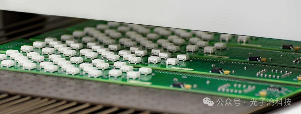
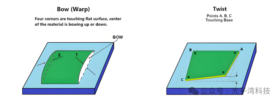
PCB warping is a common issue during the manufacturing process of printed circuit boards, caused by various factors during manufacturing and processing, which can be divided into thermal stress and mechanical stress. Most occur during lamination, hot air solder leveling, solder mask curing, uneven copper distribution, improper storage of process control boxes, and cutting and separation stages.
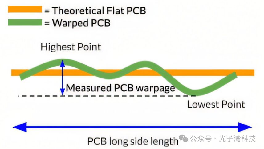
Measuring PCB warpage
This warping can lead to various issues, including component misalignment, poor solder joint quality, and even equipment failure.
PCB warping can cause many problems for electronic devices, leading to performance degradation and reliability issues, and in severe cases, even complete failure.
The glass transition temperature (Tg) between layers and the coefficient of thermal expansion (CTE) mismatch can generate excessive stress during the lamination process, causing warping.
The following are potential hazards of PCB warping:
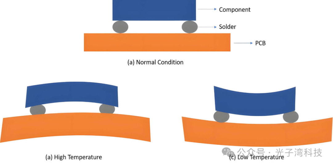
Severely warped PCBs may suffer physical damage during assembly or operation. Components may detach from solder joints. Over time, warping of PCBs may lead to fatigue failure of solder joints, traces, or even the PCB laminate itself.
When components are soldered onto a warped PCB, they may lose mechanical and electrical contact with the PCB. This can affect performance, increase the resistance of electrical connections, and lead to solder joints overheating over time.
-
Electromagnetic Interference:
Air gaps created by warped PCBs can lead to electromagnetic interference (EMI), affecting circuit performance. The immunity of components to external sources of EMI may be reduced.
For PCBs used in applications with forced convection cooling (fans), severe warping can obstruct or change the airflow direction, thereby reducing the ability of heat sinks and other cooling elements to dissipate heat from components. This can lead to overheating and component damage/failure.
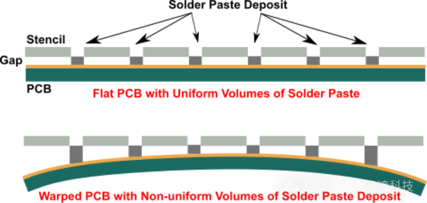
The amount of solder paste deposited on the PCB is uneven due to warping.
IPC standards specify acceptable levels of PCB warping, including: IPC-6011: General Performance Specification for Printed Circuit Boards, IPC-6012: Qualification and Performance Specification for Rigid Printed Circuit Boards. According to IPC-6012 standards, the maximum allowable warpage for SMT PCBs is 0.75%, while the maximum warpage for other types of PCBs is 1.5%. These standards are designed to ensure reliability requirements are met during manufacturing and assembly. Compared to IPC-RB-276 standards, IPC-6012 has stricter requirements for SMT PCBs.
 In actual production, most PCB assembly factories require warpage for double-sided or multilayer PCBs (thickness 1.6mm) to be 0.70%~0.75%, while for BGA packages and other precision applications, the warpage requirement is generally reduced to 0.5%, and some factories may even raise the requirement to 0.3% to ensure manufacturing precision and reliability. Manufacturers should specify the required IPC level for their PCBs based on intended use and reliability requirements.
Maintaining proper design, material selection, process control, and handling procedures helps to minimize warping and produce high-quality PCBs. Through careful optimization, warping can often be reduced to acceptable industry standards.
Application of 3D Confocal Microscopy in PCB Inspection
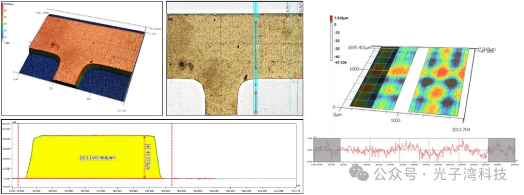
By performing repeated measurements at multiple locations of the same target, automated measurements, and creating OK/NG templates, warping detection of PCBs and PCB-mounted components is conducted, with high-color display making the warping phenomena visible.
At the same time, we also support inspection of pattern height and cross-sectional area on PCB, as well as detection of surface roughness of metal-plated patterns.
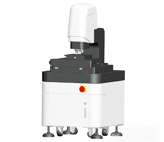
Meinuo Photonics 3D Confocal Microscope
Technical Support: 199-6293-0018
Meinuo Photonics3D Confocal Microscope is a device used for various precision components and material surfaces, capable of addressing diverse measurement scenarios, efficiently completing sub-micron level morphology and surface roughness measurement tasks, providing reliable high-quality data.
-
Ultra-wide field of view, high-resolution color image observation
-
Provides five major analysis functions: roughness, geometric profile, structure, frequency, and function
-
Adopts a pinhole confocal optical system with a highly stable structural design
-
Provides four major data processing functions: position adjustment, correction, filtering, and extraction
With the continuous development of electronic technology, PCB design and manufacturing technologies are also advancing to meet the demands for higher speeds, smaller sizes, and higher performance.Meinuo Photonics 3D Confocal Microscope applications provide an efficient and precise solution for detecting PCB warping issues. Through this technology, we can identify and correct warping issues during the production process, thereby enhancing product reliability and performance.
*Special Statement: The original and reprinted articles published by this public account are for academic sharing and conveying industry-related information only. Without authorization, any acts of plagiarism, alteration, citation, reprinting, etc., that infringe upon the rights of this public account are prohibited. The content is for reference only; if copyright issues arise, please contact us, and we will verify and handle it promptly.


