Understanding Gigabit Ethernet Bandwidth Limitations

Introduction

With the growing demand for networking, the issue of gigabit Ethernet speed has garnered significant attention. This article analyzes the low actual speed situation, detailing reasons such as poor wiring, and provides effective methods for improving speed and stability from both hardware aspects like equal-length wiring and impedance matching, as well as software debugging perspectives.
The theoretical speed of normal gigabit Ethernet can reach 1000Mbps, but considering losses in various communication links, it should be above 800Mbps. However, many boards, following reference circuit designs, only achieve actual speeds of 300/400Mbps or even lower. This situation is 90% due to poor Ethernet wiring leading to signal integrity issues.
The speed of gigabit Ethernet RGMII signals reaches up to 125MHz and is triggered on both edges, which imposes requirements on signal integrity. The following principles and methods for RGMII signal integrity can help optimize and improve Ethernet speed and stability.
1. Equal-Length Wiring
RGMII requires equal-length processing during wiring. Equal length means that the six signals in the RGMII bus, TX_CLK, TXD[0:3], and TX_EN form one group, while RX_CLK, RXD[0:3], and RX_EN form another group. These should be routed in a serpentine manner, ensuring that the length difference between the signals in each group is within 100mil. Different manufacturers may have varying tolerance requirements, but for hardware engineers, the smaller the tolerance, the larger the timing margin, and efforts should be made to minimize tolerances when designing. Note that this tolerance should be calculated from the CPU’s MAC to the PHY chip wiring. Some core board manuals specify the RGMII wiring length of the core board and the internal length of the CPU, so these must be summed with the baseboard length for equal length calculations.
2. Impedance Matching
All signal lines in RGMII require single-ended 50Ω impedance matching. The 50Ω value is a convention that has been used to this day and is familiar to board manufacturers, making it easy to layer and produce boards. Impedance matching refers to the characteristic impedance, which is defined as the impedance of the transmission line when the length approaches infinity (for example, the aforementioned 50Ω). In finite-length transmission lines, it characterizes the instantaneous impedance of the electrical signal passing through the conductor, but this value is not 50Ω. Impedance matching means that the characteristic impedance at every point in the finite-length transmission line is equal, uniform, and continuous. During design, it is calculated based on the PCB’s copper thickness, line width, inter-layer spacing, and board material.
For designers, the most important factor is the continuity of impedance. When electrical signals pass through conductors with discontinuous impedances, it is like light passing through media of different densities (water and air), causing reflection and refraction, which distorts the signal. Through-holes, layer changes, passing through resistors and connector pads, and branching can all lead to varying degrees of impedance discontinuity. Therefore, during layout, avoid branching and change directions using 45-degree bends, and minimize through-holes for layer changes.
3. Complete Reference Plane
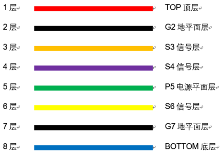
The reference plane is crucial for impedance matching. According to transmission line principles, a transmission line consists of signal lines and return paths. When the signal lines are uniform and continuous, but the reference plane is not, it can also lead to transmission line discontinuity. The reference plane is determined by the layering, typically being adjacent plane layers. For example, in an 8-layer board, layer 1 and layer 3 reference layer 2, layer 4 references layer 5, and layer 6 and layer 8 reference layer 7. The copper area of the reference layer within the projection area of the signal line must not be interrupted or change the network. Problematic areas often arise when changing layers; if a signal transitions from layer 1 to layer 8, the reference layer changes from layer 2 to layer 7. It is recommended to create a return path by adding ground vias within a 200mil range at layer change locations. In places where conditions allow, ground vias should also be added to enhance the continuity of the two ground layers. What if the signal changes from layer 1 to layer 4, with the reference layer changing from GND to PWR, altering the network? In such cases, it is advisable to place a 0.1uF decoupling capacitor near the layer change location to connect the networks of layers 2 and 5.
Understanding Gigabit Ethernet Bandwidth Limitations
Figure 1: A common 8-layer board stacking structure diagram
4. Avoid Source Reflection
As previously mentioned regarding impedance matching, when the signal reaches the receiving end, the RGMII receiving IO is high impedance, causing the signal to reflect back. The reflected wave reaches the source and undergoes secondary reflection, known as source reflection. Source reflection combines with the original signal, resulting in overshoot, ringing, and other issues that affect signal quality. By placing a series source matching resistor near the signal sending end, source reflection can be effectively reduced. Some chips recommend matching resistors of 33Ω, while others suggest 22Ω, due to the differing output impedances of the chip drivers. When the output impedance of the driver plus the source matching resistor is around 50Ω, combined with 50Ω impedance matching, the effect of preventing source reflection is optimal, which is why the series resistance should be close to the signal source end.
5. Prevent Crosstalk
External interference should not be ignored. Check whether there is a 3W spacing maintained between wires, and whether clock wires are grounded. In layering similar to Figure 1.44, check whether the traces on layers 3 and 4 have long-distance or close-distance parallel traces with other traces on adjacent layers, etc. These areas often reveal optimization points.
6. Software Delay Line Debugging
If the board debugging reveals insufficient speed, it may not necessarily be a hardware issue; first, check whether the software has configured the Delay line.
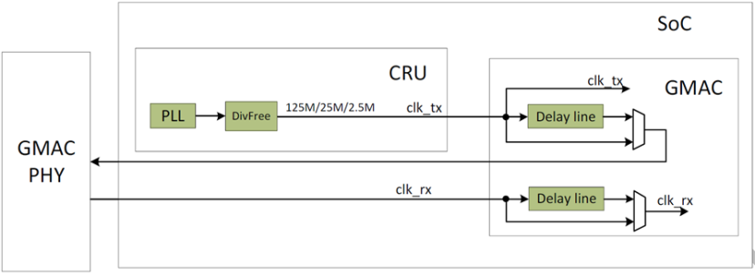
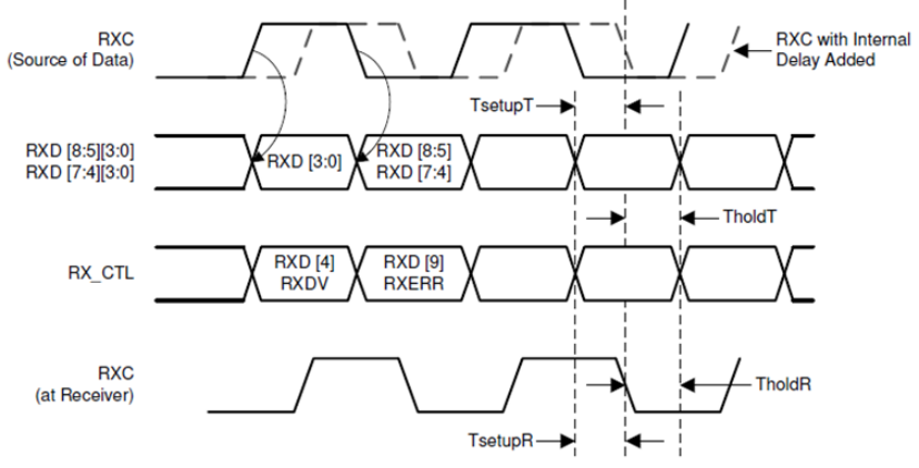
The Delay line involves adding a segment of useless buffer to the CLK to achieve a delay effect. By adjusting the number of buffers, the delay of the PCB wiring can be compensated, ultimately aligning the clock edges received at the receiving end with the center of the data eye diagram. Typically, both the MAC and PHY ends can adjust the Delay line, but the MAC end allows for finer adjustments and is more convenient to operate. Generally, the PHY end’s Delay line is set to 0, with adjustments made only at the MAC end.
Understanding Gigabit Ethernet Bandwidth Limitations
Figure 2: Delay line circuit structure diagram
Understanding Gigabit Ethernet Bandwidth Limitations
Figure 3: Delay line adjustment waveform diagram
When initially adjusting the Delay line, the network may not be reachable at all, making it difficult to distinguish whether the issue lies with sending or receiving. Therefore, it is advisable to use Wireshark on the PC side to debug the sending data.
The MAC end adjusts the Delay line with each step increasing the delay by 0.08ns. The board under test pings the PC’s IP in the background, and the command is input to have the board traverse all TX Delay lines. During this time, observe the Wireshark on the computer side, where ICMP packets sent from the board will start being received from a certain value, marking the beginning of the window. As the TX delay line gradually increases, the received packets will become more complete, then incomplete, and finally, the board will stop sending ICMP packets altogether. The TX Delay line value at this point is considered the end of the window. The average of the start and end values will be taken as the optimal TX Delay line value for this PCB board, which should be recorded.
Once the board’s network card sending function is debugged successfully, the board will be capable of responding to ping ICMP packets. Next, bind the board’s network card MAC address and IP address on the computer side, and start pinging the board’s IP address while executing the following command to traverse all RX Delay lines. Observe the return information from the ping command on the computer side, where you will see ping failures gradually change to successes, and then back to failures again. Record these corresponding RX Delay line values. The successful ping interval is referred to as the receiving window, and the middle value of this range will be taken as the optimal RX Delay line value. Finally, set the optimal Delay line value and add it to the device tree’s gmac node to solidify the Delay line configuration.
It is important to note that when using the RGMII interface to connect to a gigabit PHY, if there are hardware differences, the Delay line configuration must be redone.
Additionally, adjusting the Delay line does not imply that hardware does not need to follow equal-length layout principles. If equal-length layout is not done, it means that the clock signal’s rising edges must be adjusted for phase delay across the four data lines simultaneously. The overlapping area must allow for correct data sampling, but this area will become too narrow, potentially exceeding the Delay line’s delay range.
7. Adjusting Drive Strength
In addition to configuring the Delay line, adjusting the drive strength of RGMII can further improve issues. When using iperf for long-duration tests, if drops occur, adjusting the drive strength can be a viable solution.
Increasing the drive strength makes the signal edges steeper, but at the same time, overshoot and ringing may increase. Conversely, reducing the drive strength results in slower signal edges but can minimize the impact of overshoot and ringing. Drive strength typically has only a few levels (usually 4 or 8), with some manufacturers specifying mA values, while others only indicate strength levels without specific units. Therefore, it is not necessary to find an optimal value like with the Delay line; practical testing under different strengths will yield the highest rate and best stability.
Understanding Gigabit Ethernet Bandwidth Limitations
  • AM335x Upgrade Option

  • Dual Gigabit Ethernet

  • Three CAN FD Channels

  • Supports GPMC

Reference Price: Starting from 319 Yuan

Understanding Gigabit Ethernet Bandwidth Limitations

Long press to purchase

Understanding Gigabit Ethernet Bandwidth Limitations

Leave a Comment