Source: Semika
Original Author: Semika
Integrated circuits are a collection of electronic components: resistors, transistors, capacitors, etc., all packed into a small chip and connected together to achieve a complex functional goal. They have many functional categories: circuit logic gates, operational amplifiers, timers, voltage regulators, circuit controllers, logic controllers, microprocessors, memory and so on.
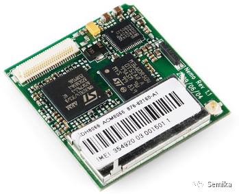
Integrated circuits (ICs) are the cornerstone of modern electronic technology. They are the heart and brain of most circuits. They are everywhere, and you can find them on almost every circuit board. Therefore, it is very important to recognize and understand these chips.
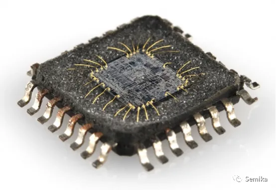
When we imagine what a chip looks like, the first thing that comes to mind might be a small black square, like the one below. But what is inside that black box? It can be difficult to form an image of that in the mind.
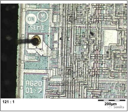
The inside of the chip is a complex circuit structure made up of silicon wafers, copper, and other materials, interconnected to form resistors, capacitors, transistors, or other components in the circuit. Chips are initially made on round silicon wafers, and after the circuit is completed, the wafers are cut into small pieces to form chips.
The chip itself is very small, and the semiconductor wafers and copper layers are very thin. The connections between the layers are very complex.The image below is a close-up of the inside of a chip:
Once formed, the chip is the smallest unit of an application circuit. Because the chip is too small to be soldered or connected directly, chip packaging technology is needed to facilitate the connection of the circuit to the chip. Chip packaging technology transforms the delicate small silicon wafer into the black chips we are all familiar with.
Packaging technology creates the finished product of the chip and expands it into a structure that is easier to connect with other circuits.Each external connection on the chip is connected to pads or pins on the package via a small gold wire.The pins are silver extruded terminals on the chip circuit that continue to connect to other parts of the circuit.
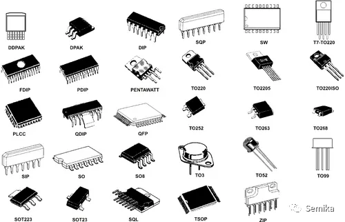
There are many different types of packaging, each with unique sizes, mounting types, and pin counts. The image below lists dozens of chip packaging methods, each with its unique name. Some of the major packaging categories will be explained in detail later.
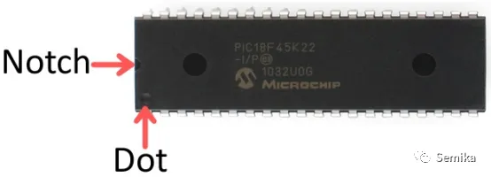
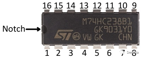
Polarity Marking and Pin Numbering
All chips have polarity markings, and the position and function of each pin are unique. This means that the packaging must have some way to define the function of each pin. Most chips will use a notch or a dot to indicate which pin is the first pin (sometimes both).
Once you know where the first pin is, the remaining pin coding is done by increasing counter-clockwise in order around the chip.
One of the main distinguishing features of chip packaging types is how they are mounted to the circuit board. All packages belong to one of two mounting types: Through-Hole (PTH) or Surface Mount (SMD or SMT). Through-hole packages are generally larger and easier to use. They are designed to pass through one side of the circuit board and then be soldered to the other side.
Surface mount packages are designed to be located on the same side of the circuit board and soldered to the surface of the board. SMD package pins come in two types: one is led out from the side, perpendicular to the chip; the other is located at the bottom of the chip, arranged in a matrix. This type of component is less “suitable for hand assembly”. They usually require special tools to assist in the process.
Next, we will provide detailed visual explanations of various common chip packaging types to help you remember their names and appearances.
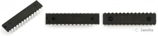
4.1 Dual In-line Package (DIP)
(DIP: Dual In-line Package)
DIP is the most common through-hole IC package. These small chips have two rows of parallel pins extending vertically from a rectangular black plastic housing.
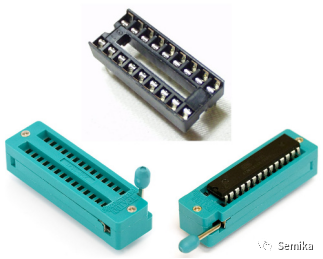
In addition to being soldered directly to the integrated circuit, a chip socket can also be used. Using a socket allows DIP ICs to be removed and swapped, making it easy to replace if the chip happens to burn out.
4.2 Surface-Mount (SMD/SMT)
(SMD/SMT: Surface-Mount)
There are now a variety of surface-mount packaging types. Typically, a wiring pattern matching the chip must be pre-made on the PCB and soldered onto it. SMT installations usually require automated equipment.
4.3 Small Outline Package (SOP)
(SOP: Small Outline Package)
SOP packaging is the evolutionary form of DIP’s surface mount. If all the pins on a DIP are bent outward and then reduced to a suitable size, a single-sided installed SOP can be formed. This packaging is one of the easiest SMD components to solder by hand. In SOIC (Small-outline IC) packaging, the distance between each pin is typically about 0.05 inches (1.27 mm).
SSOP (Shrink Small Outline Package) is a smaller version of SOIC packaging. Other similar IC packages include TSOP (Thin Small Outline Package) and TSSOP (Thin-Shrink Small Outline Package).
4.4 Quad Flat Package (QFP)
(QFP: Quad Flat Package)
In the QFP, the IC pins extend in all four directions, looking like a quad flat package (QFP). QFP ICs can have 8 pins on each side (32 total) to 70 pins (over 300 total). The pin spacing on QFP ICs typically ranges from 0.4mm to 1mm. Standard QFP has some miniaturized variations, including thin QFP (TQFP), very thin QFP (VQFP), and low-profile QFP (LQFP) packaging.
4.5 Quad Flat No-leads (QFN)
By removing the pins from the QFP IC and shrinking them to the edges of the four corners, you get something that looks like a Quad Flat No-leads (QFN) package. The connections on QFN packages are much smaller, exposed at the edges of the IC bottom.
Thin (TQFN), ultra-thin (VQFN), and micro-lead (MLF) packages are variants of the standard QFN package. There are also dual no-leads (DFN) and thin dual no-leads (TDFN) packages, where the pins are only on two sides.
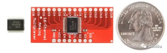
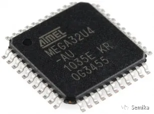
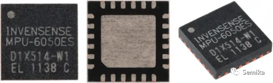
Many microprocessors, sensors, and other new ICs use QFP or QFN packaging. The popular ATmega328 microcontroller offers TQFP packaging and QFN (MLF) form, while micro accelerometers/gyroscopes like the MPU-6050 use a micro QFN form.
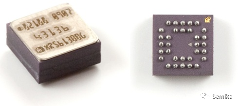
4.6 Ball Grid Arrays (BGA)
(Ball Grid Arrays)
Finally, for truly advanced integrated circuits, there are Ball Grid Array (BGA) packages. This is a complex and delicate packaging, where small solder balls are arranged in a two-dimensional grid at the bottom of the IC. Sometimes the solder balls are directly attached to the chip!
BGA packaging is typically used on advanced microprocessors.
If you can hand-solder a BGA packaged IC, you can consider yourself a master-level solderer. Typically, placing these packages on a PCB requires an automated process, including pick-and-place machines and reflow ovens.
Integrated circuits are ubiquitous in electronic products in various forms, making it difficult to cover everything. Below are some of the more common ICs you might encounter in electronic products.
5.1 Logic Gates, Timers, Shift Registers, etc.
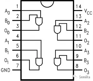
Logic gates, as building blocks of more integrated circuits, can be packaged into their own integrated circuits. Some logic gate ICs may contain a small number of gates in one package, such as this four-input AND gate:
Logic gates can be connected within integrated circuits to create timers, counters, latches, shift registers, and other basic logic circuits. Most of these simple circuits can be found in DIP packages, as well as SOIC and SSOP.
5.2 Microcontrollers, Microprocessors, FPGAs, etc.
Microcontrollers, microprocessors, and FPGAs are all integrated circuits that package thousands, millions, or even billions of transistors into a small chip. These components are complex in function and vary greatly in size. From 8-bit microcontrollers, such as the ATmega328 in Arduino, to complex 64-bit multi-core microprocessors, these are widely used components in computers.
These components are often also the largest integrated circuits in the circuit. Simple microcontrollers can be found in packages ranging from DIP to QFN/QFP, with pin counts ranging from 8 to 100. As the complexity of these components increases, the packaging also becomes more complex. FPGAs and complex microprocessors can have over a thousand pins and are only used in advanced packages such as QFN, LGA, or BGA.
5.3 Sensors
Modern digital sensors, such as temperature sensors, accelerometers, and gyroscopes, are all integrated into an integrated circuit.
These ICs are typically smaller than microcontrollers or other ICs on the circuit board, with pin counts ranging from 3 to 20. Many large control chips also integrate many sensors directly inside.
END
The reproduced content reflects only the author’s views
It does not represent the position of the Institute of Semiconductors, Chinese Academy of Sciences
Editor: March
Responsible Editor: Six Dollar Fish
Submission Email: [email protected]
1. The Institute of Semiconductors has made progress in research on bionic cover-type neuron models and learning methods
2. The Institute of Semiconductors has made significant progress in inverted structure perovskite solar cells
3. Why do chips use copper as interconnect metal?
4. What exactly is the 7nm technology in chips?
5. Silicon-based integrated photonic quantum chip technology
6. How anomalous is the quantum anomalous Hall effect? It may lead to the next revolution in information technology!