Understanding Automotive Camera Technology, Market, and Future Prospects

Introduction:

This article is published with permission from A Bao 1990, the author is A Bao 1990.

The automotive camera is known as the “eye of autonomous driving”. It mainly collects image information through lenses and image sensors. In recent years, cameras have become one of the most common intelligent tools in automotive vision solutions. In this article, let’s explore the past and present of automotive cameras.

1

Pinhole Imaging

In the early Warring States period, Chinese scholar Mozi (468 BC – 376 BC) and his disciples completed the world’s first experiment on pinhole imaging, recorded in the “Mo Jing”: “The scene arrives, at noon there is an end, and the scene is long. It is said to be at the end. “The scene. The light of the person is like shooting, the lower one is high; the higher one is low. The foot blocks the lower light, so the scene is formed above; the head blocks the upper light, so the scene is formed below. There are ends in the distance and near, and with the light, the scene is in the library.”
This article explains the reason for the inverted image of the pinhole and points out the nature of light propagation in a straight line. This was the first scientific explanation of the straight line propagation of light.
In the Western world, it wasn’t until 350 BC that the ancient Greek scholar Aristotle proposed the laws of optics, and from then on, Westerners understood the optical principles of pinhole imaging.
Understanding Automotive Camera Technology, Market, and Future Prospects

2

Camera Obscura

At the end of the 15th century, people created the camera obscura based on the principle of pinhole imaging, which is essentially the prototype of the camera. Italian Leonardo da Vinci described this camera in his writings, detailing how people used this tool to sketch and paint.
In 1553, Italian Porta published a book titled “Natural Magic” that extensively introduced the use of the camera obscura. Using this tool, one could simply use a pencil to reflect the image on paper, outline the shape, and then color it to complete a highly realistic portrait that accurately matched reality.
Understanding Automotive Camera Technology, Market, and Future Prospects

3

Silver Plate Photography

In 1822, Frenchman Niepce produced the world’s first photograph on photosensitive material, but the image was not very clear and required 8 hours of exposure. In 1826, he took the earliest existing photo on a tin base coated with photosensitive asphalt using a camera obscura.
In 1838, French physicist Daguerre invented the daguerreotype method, which used a silver iodide-coated steel plate for exposure in a camera obscura, then developed with mercury vapor and fixed with regular table salt. The result was essentially a metal negative, but it was very clear and could be preserved permanently. Subsequently, Daguerre created the world’s first camera using this method, requiring an exposure time of 20 to 30 minutes.
On August 19, 1839, the French government announced the abandonment of the patent for the silver plate photography invention and made it public. This day is generally regarded as the beginning of photography.
Understanding Automotive Camera Technology, Market, and Future Prospects

4

Film Cameras & Digital Cameras
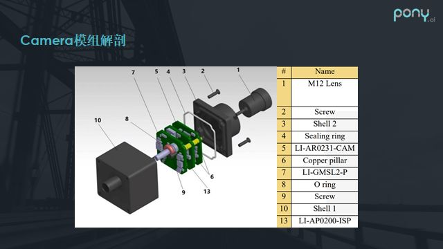
In 1866, German chemist Schott and optician A. G. invented barium crown optical glass at Zeiss, resulting in the rapid development of the design and manufacturing of photographic lenses.
With the development of photosensitive materials, in 1871, dry plates made of silver bromide photosensitive material appeared, and in 1884, film made of nitrocellulose was introduced.
In 1888, Kodak produced a new type of photosensitive material—a soft, rollable “film”. This was a leap in photosensitive materials. In the same year, Kodak invented the world’s first portable box camera equipped with film. Kodak No.1 was launched as a household camera, and its slogan was “Press the shutter, and I will do the rest.” This camera can be said to be the ancestor of consumer cameras.
Understanding Automotive Camera Technology, Market, and Future Prospects
In 1969, the CCD chip was applied in the cameras mounted on the Apollo lunar module in the United States, laying the technical foundation for the electronicization of photographic materials.
In 1981, Sony produced the world’s first camera using a CCD electronic sensor as the photosensitive material after years of research, laying the foundation for electronic sensors to replace film. Following that, Panasonic, Copal, Fuji, and several electronic chip manufacturers from the United States and Europe invested in the R&D of CCD chip technology, laying the technical foundation for the development of digital cameras.
In 1987, cameras using CMOS chips as photosensitive materials were born at Casio.
Understanding Automotive Camera Technology, Market, and Future Prospects
Looking back at the development history of cameras:
Understanding Automotive Camera Technology, Market, and Future Prospects

5

Explanation of Camera Module Internal Structure and Working Mechanism

Understanding Automotive Camera Technology, Market, and Future Prospects
Lens: Gathers light and projects the scene onto the imaging medium. Some are single lenses, while others require multi-layer glass for better imaging effects.
Filter: The visible light spectrum seen by the human eye is limited, while the light spectrum that the image sensor can recognize is much larger. Therefore, a filter is added to remove excess wavelengths, allowing the image sensor to capture the actual scene seen by the human eye.
Image COMS sensor chip: The imaging medium converts the image (light signal) projected by the lens into an electrical signal.
Circuit board substrate: Transmits the electrical signals from the image sensor to the backend. For automotive cameras, the circuit board will have more circuits to convert parallel camera signals into serial transmission, thus enhancing anti-interference capability.
Understanding Automotive Camera Technology, Market, and Future Prospects
The working principle of the camera module is that the lens gathers light, and then through the IR filter, unnecessary infrared light is filtered out. At this point, the analog signal enters the sensor COMS chip, which outputs a digital signal through AD conversion. Some cameras will place an ISP image processing chip on the camera side to transmit the processed signal to the host, while others do not place an ISP chip and use the built-in ISP chip on the host for image processing, which significantly improves heat dissipation and reduces radiation at the camera end.

6

Automotive Camera Architecture

Understanding Automotive Camera Technology, Market, and Future Prospects
The structure of the automotive camera is shown in the figure above. If placed outside the vehicle, a complete camera must be assembled. If it is a DVR inside the vehicle, waterproofing is not a concern, and it can be assembled into the camera module shown above.
Understanding Automotive Camera Technology, Market, and Future Prospects
The above image shows a common dissection of the camera module used in vehicles. Apart from the outer aluminum shell, sealing ring, and lens, the middle consists of relatively simple layered designs, usually including the sensor board, the small board for the image processor, and a serial board. Why is a serial converter needed? Because the camera sensor or ISP’s image data output bus is usually MIPI CSI standard, characterized by high-speed transmission but short transmission distances; otherwise, signal integrity cannot be guaranteed.
Therefore, in vehicles, we need to convert it to high-speed bus standards suitable for long-distance transmission, such as GMSL. Thus, the camera module typically uses a serial board for bus conversion. Additionally, coaxial cables can be used to both power the module and transmit image data.

7

Differences Between CCD and CMOS Image Sensors

CCD (Charge Coupled Device) is a photosensitive coupling component primarily made of silicon semiconductor. Its basic principle is similar to the solar cells on a CASIO calculator, where through the photoelectric effect, the photosensitive component’s surface senses the incoming light and converts it into the ability to store charge. In simple terms, when the CCD surface receives light during the opening of the shutter, it converts the light energy into charge, with stronger light producing more charge. These charges become the basis for determining the intensity of the light.
CMOS (Complementary Metal-Oxide Semiconductor) uses silicon and germanium as its main materials, allowing N (negative charge) and P (positive charge) semiconductors to coexist on the CMOS. The current produced by these two complementary effects can be recorded and interpreted by the processing chip.
Understanding Automotive Camera Technology, Market, and Future Prospects
The biggest difference between CMOS and CCD lies in the position and number of amplifiers. Comparing the structures of CCD and CMOS, the position and number of amplifiers are the most significant differences.
Understanding Automotive Camera Technology, Market, and Future Prospects
Each time CCD is exposed, after the shutter closes or the internal frequency automatically disconnects (electronic shutter), it processes pixel transfer, sequentially transferring the charge signal from each pixel in each row to the “buffer” (charge storage) and outputting it to the amplifier next to the CCD for amplification, then passing through the ADC (analog-to-digital converter) for output.
Understanding Automotive Camera Technology, Market, and Future Prospects
In CMOS design, each pixel is directly connected to an “amplifier,” allowing the photoelectric signal to be amplified before being moved to the ADC for conversion into digital data. Due to structural differences, CCD and CMOS exhibit different performance characteristics. CCD is characterized by maintaining signal integrity during transmission (dedicated channel design), collecting all pixel signals to a single amplifier for unified processing, thus preserving data integrity. In contrast, CMOS’s simpler process lacks a dedicated channel design, requiring amplification before integrating data from various pixels.
Understanding Automotive Camera Technology, Market, and Future Prospects
1. Sensitivity differences: Due to the presence of amplifiers and A/D conversion circuits in each CMOS pixel, excessive additional devices compress the light-sensitive area of a single pixel, resulting in lower brightness sensitivity compared to CCD with the same pixel size.
2. Resolution differences: As mentioned in the sensitivity difference, due to the more complex structure of each CMOS pixel, its light-sensitive aperture is smaller than that of CCD, meaning that for the same size sensors, CCD’s resolution is generally superior to that of CMOS. However, if we step outside size constraints, CMOS sensors can achieve designs of up to 14 million pixels/full-frame, overcoming manufacturing difficulties associated with larger sensors.
3. Noise differences: Since each photo-sensitive diode in CMOS is paired with an ADC amplifier, when calculated for millions of pixels, over a million ADC amplifiers are needed. Although these products are manufactured uniformly, each amplifier has slight variations, making it challenging to achieve synchronized amplification. In contrast, CCD, with a single amplifier, typically results in lower noise.
4. Power consumption differences: The image charge driving method in CMOS is active, meaning that the charge generated by the photo-sensitive diode is directly amplified and output by the adjacent transistor. In contrast, CCD operates passively, requiring external voltage to move charges from each pixel into transmission channels. This external voltage typically needs to exceed 12 volts, necessitating more precise power line designs and voltage tolerance, resulting in much higher power consumption in CCD compared to CMOS.
5. Cost differences: CMOS uses semiconductor manufacturing processes common in the industry, allowing for the integration of all peripheral facilities onto a single chip, reducing the cost burden of chip processing and yield loss. In contrast, CCD, which outputs information through charge transfer, must create separate transmission channels, and if one pixel fails (Fail), it can block the signals of an entire row. Consequently, CCD’s yield is lower than that of CMOS, and the additional need for transmission channels and external ADCs make CCD’s manufacturing costs higher than those of CMOS.
6. Other differences: Individual Pixel Addressing (IPA) is commonly used in digital zoom. CMOS must rely on x and y positioning for zoom processing; otherwise, errors in individual pixel amplifiers can easily cause uneven images. In production, CCD requires specially customized equipment to manufacture, while CMOS can use standard memory or processor equipment for production.

8

Analysis of CMOS Sensor Composition and Key Parameters

The function of the image sensor is photoelectric conversion. Key parameters include pixel count, individual pixel size, chip size, and power consumption. Technological processes include front-illuminated (FSI), back-illuminated (BSI), and stacked (Stack). Below is a brief introduction.
Understanding Automotive Camera Technology, Market, and Future Prospects
The image sensor is externally visible, consisting of the light-sensitive area (Pixel Array), bonding pads, internal circuits, and substrate. The light-sensitive area is a single pixel array made up of multiple individual pixel points. When the light signals captured by each pixel are combined, they form a complete image.
Understanding Automotive Camera Technology, Market, and Future Prospects
CMOS chips consist of micro-lens layers, color filter layers, circuit layers, photosensitive element layers, and substrate layers.
Understanding Automotive Camera Technology, Market, and Future Prospects
Cross-section of a CMOS chip
Due to the varying angles of light entering each pixel, a micro-lens is added to correct the light angle at each pixel’s surface, ensuring that light enters the photosensitive element surface perpendicularly. This is the concept of chip CRA, which must be kept within a certain deviation range from the lens’s CRA.
Understanding Automotive Camera Technology, Market, and Future Prospects
In terms of circuit architecture, we add an image sensor as a black box that converts light signals into electrical signals. The external components usually include power, data, clock, communication, control, and synchronization circuits. It can be simply understood that the light-sensitive area (Pixel Array) converts light signals into electrical signals, and the logic circuits within the black box process and encode these electrical signals before outputting them via data interfaces.
Understanding Automotive Camera Technology, Market, and Future Prospects

9

Key Parameters of Image Sensors

1. Pixel: Refers to the number of individual pixel points within the light-sensitive area, such as 5 Megapixels, 8 Megapixels, 13 Megapixels, 16 Megapixels, 20 Megapixels. The more pixels, the larger the captured image area, and the more details can be captured.
2. Chip size: Refers to the diagonal distance of the light-sensitive area, usually expressed in imperial units, such as 1/4 inch, 1/3 inch, 1/2.3 inch, etc. The larger the chip size, the higher the material cost.
3. Individual pixel size: Refers to the length and width dimensions of a single photosensitive element, also known as the aperture size of a single pixel, such as 1.12 micrometers, 1.34 micrometers, 1.5 micrometers, etc. The larger the aperture size, the greater the amount of light energy entering per unit time, resulting in higher overall performance of the chip and better overall image quality. Individual pixel size is a critical parameter for image sensors.
Understanding Automotive Camera Technology, Market, and Future Prospects
Front-Illuminated (FSI) and Back-Illuminated (BSI)
The traditional CMOS image sensor is structured in a front-illuminated manner, with the lens layer, color filter layer, circuit layer, and photosensitive element layer arranged from top to bottom. When using this structure, light must pass through the openings in the circuit layer to reach the photosensitive element layer, which can lead to light loss.
In contrast, back-illuminated structures place the photosensitive element layer above the circuit layer, retaining only the necessary logic circuits for the photosensitive layer. This allows light to enter the photosensitive element layer more directly, reducing light loss, such as reflection. Therefore, in the same unit of time, the amount of light energy that a single pixel can capture is larger, resulting in a significant improvement in image quality. However, the production process for this structure is more complex, leading to lower yields and relatively higher costs.
Understanding Automotive Camera Technology, Market, and Future Prospects
CMOS chips have various key parameters, including pixel count, individual pixel size, chip size, and power consumption. In terms of technology, there are front-illuminated (FSI), back-illuminated (BSI), and stacked (Stack) types. Below is a brief introduction.
Understanding Automotive Camera Technology, Market, and Future Prospects
Image sensors consist of various components, including lenses, filters, image sensors, and circuit boards. The image processing and data transmission systems are crucial for ensuring high-quality image capture and processing in automotive applications.

45

Conclusion

In summary, automotive camera technology is rapidly evolving, driven by advancements in image processing, sensor technology, and the growing demand for autonomous driving applications. Understanding the principles of camera operation, sensor characteristics, and the integration of these systems is essential for the future of automotive technology.

Leave a Comment

×