Click
Subscribe to the “IEEE Electrical and Electronics Engineers Society” public account above. Gather global technological frontier dynamics and open up your mind for scientific research and entrepreneurship.

━━━━
This is 2028. Wednesday at 8 PM, you are starving. You stare at the only food left in the fridge: a pack of unappetizing gray sausages. Was it always like this? Can it still be eaten safely? In 2018, you could only rely on your sense of smell to take a gamble. But in 2028, you just need to shake your smartphone above the packaging. The smartphone will inquire with the embedded sensor in the packaging, which can measure the gas concentration related to meat decomposition. The smartphone will display the message “Safe to eat within the next 20 hours,” and then provide a sausage cooking recipe. You are so hungry that you don’t even have time to look at the recipe, just tearing open the package and tossing the sausages into the frying pan, discarding its packaging and the high-tech sensor.
This fictional scenario saved by the smartphone is just one of the many applications that the Internet of Things (IoT) may present. The integration of low-cost, low-power components, especially microprocessors, cellular radios, Wi-Fi radios, and micro-electromechanical systems (MEMS) sensors, has made the IoT possible today. In addition, the IoT data that aggregates consumer behavior (i.e., big data) is also a validated market. The research firm IHS Markit, tracking and analyzing the electronics industry, predicts that the number of IoT devices worldwide will grow more than fourfold, from 27 billion in 2017 to 125 billion by 2030.
To say this will stimulate the semiconductor industry is not entirely accurate. This stimulation is based on an important assumption—that all these components will use silicon, utilizing the existing $10 billion chip factories (i.e., wafer fabs) for manufacturing. But this assumption is incorrect. Disposable sensors capable of sniffing out the future safety of sausages will not be made of silicon. Instead, they will be directly printed onto paper or plastic packaging.
━━━━
Currently, IoT application sensors are based on MEMS. MEMS sensors are made on silicon wafers using the same methods originally used to manufacture semiconductor integrated circuits, utilizing micro-mechanical structures to detect motion, sound, pressure, light, and even special gases. They respond to physical stimuli through thin films, cantilevers, vibrating bodies, or meandering paths smaller than 100 microns (equivalent to the diameter of human hair), converting them into electronic signals. Once connected to radios and antennas, MEMS sensors can wirelessly transmit electronic data to the Internet.
MEMS sensor chips typically measure only 1 or 2 millimeters, meaning thousands of chips can be economically produced on a 200-millimeter diameter silicon wafer. Currently, large-capacity MEMS sensors (such as microphones and gyroscopes) cost only $0.10 to $0.50. This makes them suitable for smartphones, fitness trackers, and other consumer electronics priced around $100.
For disposable products like food packaging, medical testing, or smart clothing costing less than $10, the cost of sensors should be reduced to just $0.01. In other words, the price of MEMS sensors needs to drop to one-tenth of their current price to be widely used in such low-cost IoT products.
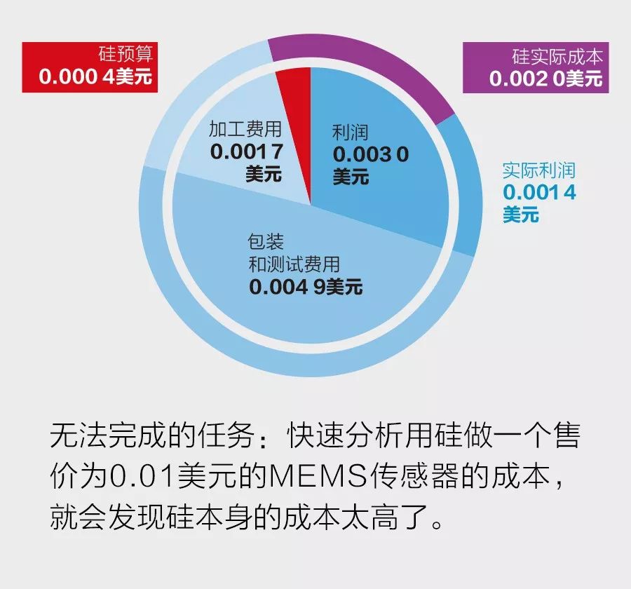
Although there is still much room for cost reduction in silicon MEMS manufacturing, it will ultimately be limited by the cost of silicon itself. Currently, a MEMS sensor made on a 200-millimeter wafer measures 1 millimeter x 1 millimeter and contains about $0.002 of semiconductor-grade silicon cost.
We can illustrate this issue with a simple math problem. (If you don’t want to see it, you can skip to the next paragraph.) If the selling price of a 1 square millimeter sensor is $0.01, then the manufacturer should not exceed $0.007 in making that sensor, as most manufacturers want to achieve at least a 30% profit margin when selling that sensor, which is $0.003 profit. According to the current rule of thumb for manufacturing sensors, the cost of MEMS chips is about 30% of the final sensor product cost, with the remaining 70% covering the sensor’s packaging, testing, electronic data reading, and calibration. Therefore, the cost of the MEMS chip can only be 30% of $0.007, which is about $0.002. Finally, silicon materials account for about 20% of the cost of unpackaged MEMS chips. This leaves a budget of only $0.0004 for the silicon used in the sensor.
In other words, to manufacture a MEMS sensor priced at $0.01, the cost of silicon needs to be only one-fifth of its current price. Looking at the historical price trend of silicon, it seems unlikely that prices will drop this much. (In fact, during the photovoltaic boom from 2006 to 2010, the price of silicon was more than ten times higher than it is now.) Shrinking MEMS chips to achieve a price target of $0.01 will not work either. Since MEMS devices rely on the mechanical properties of silicon, liquids, and gases, if they are significantly reduced in size, most MEMS devices will not function. Instead, we must manufacture sensors using materials that are much cheaper than silicon.
━━━━
In all industries, market forces always drive manufacturers to turn to low-cost materials. In automobiles, metal parts are replaced by plastics; in furniture, leather is replaced by vinyl resin; in electronics, the substrate of LEDs has shifted from sapphire to silicon.
Now, even MEMS sensors are using plastic and paper materials. Manufacturing electronic devices on these simple substrates seems to be a radical new idea, but it is not. This precedent dates back nearly 40 years, when T. Peter Brody of Westinghouse and Derrick P. Page first manufactured thin-film transistors (TFT) on paper substrates. They envisioned using precision roll-to-roll printing methods to produce electronic paper documents and implantable medical devices.
Researchers have been working on paper and plastic sensors for years, and reducing sensor costs is not their only goal. Competitive federal funding has guided researchers to explore microfabrication techniques that do not require clean rooms and special tools. Additionally, there is growing interest in using softer, biodegradable materials than silicon for invasive medical applications. As electronic products become widely used worldwide, developing countries increasingly need to use the cheapest materials—paper.
A principle of product engineering is that if you can do it with a hammer, don’t use a gold hammer. In IoT applications, flexibility, low cost, and disposability are essential, but the sensing metrics are not as strict, and plastic and paper sensors will perform excellently at an attractive price.
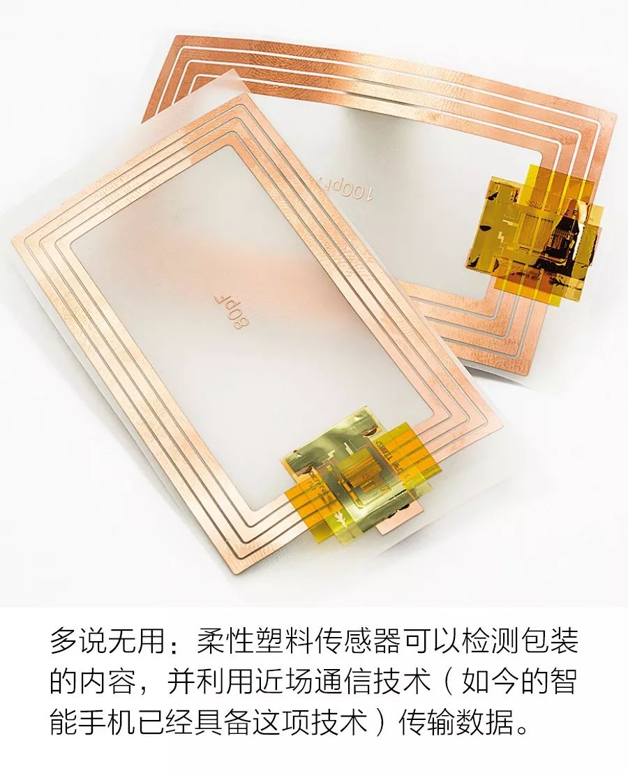
IoT sensors have two important components: one is the sensor itself, which can detect specific physical or chemical events; the other is the telemetry unit, which can transmit sensor data to the Internet. The telemetry device may not require a battery, instead relying on passive antenna coils to inductively transmit data to nearby RFID (Radio Frequency Identification) or NFC (Near Field Communication) readers. The device may also have a battery, wireless transmission device, and antenna to actively transmit data within the phone, Wi-Fi, or Bluetooth frequency range.
IoT sensors may even have some intelligence or data interpretation capability. To this end, paper-based integrated circuits made from metal and semiconductor inks are under study. In 2011, engineers at the Belgian Microelectronics Research Center (Imec) created an 8-bit microprocessor on flexible plastic using organic semiconductors. Last year, they studied a printed plastic NFC chip using a metal oxide semiconductor IGZO made from a mixture of indium, gallium, zinc, and oxygen. Although these designs are still quite primitive and slow compared to silicon materials, and may not make significant progress due to the limitations of the materials themselves, they have already proven capable of performing the job at a suitable price.
However, most IoT sensors, especially cheap disposable sensors, will rely on external power and intelligence. Both methods are very common. For example, all new smartphones can perform near-field communication, primarily used for contactless electronic payment systems like Apple Pay. This means your phone may already have the capability to power and communicate with future sausage freshness sensors.
━━━━
You can see the shift towards flexibility and biodegradability. The first approved MEMS pressure sensors for implantation by the U.S. Food and Drug Administration include one manufactured by CardioMEMS (now part of St. Jude Medical), which is a rigid sensor made of quartz that can be implanted near a stent to monitor the stent’s effectiveness in keeping the artery open. The sensor includes an antenna embedded in quartz and a quartz membrane covering a cavity, forming a capacitor. When blood pressure compresses the membrane, the capacitance changes, thereby altering the resonant frequency of the sensor circuit. The frequency change can be passively measured by an external reader, which queries the sensor with a radio frequency signal of known frequency and then compares it with the returned signal frequency that has changed.
The problem with quartz and silicon-based sensors is that they are relatively rigid and very brittle. A better choice is flexible materials that can conform to body contours and fit into narrow spaces, such as within blood vessels. Biodegradable materials are an even better choice, as they can harmlessly dissolve in the body after the sensor has completed its work, eliminating the need for surgical removal.
Subsequently, one of the co-founders of CardioMEMS, Mark Allen of the University of Pennsylvania, stopped manufacturing rigid silicon and quartz sensors and turned to producing flexible biodegradable sensors. Graduate students in Allen’s team are designing sensors and batteries made from polymers such as polylactic acid (PLGA), polyvinyl alcohol (PVA), and polycaprolactone (PCL), which are also used for dissolvable surgical sutures. Signal connection wires and antennas are made of biodegradable metals such as magnesium or zinc. Using MEMS microfabrication techniques such as photolithography and electroplating, students have developed millimeter-sized, biodegradable pressure sensors with the same wireless data transmission capabilities as quartz sensors.
Beyond the medical field, the application of biodegradable sensors is also exciting. They are highly attractive for any environmentally sensitive activities (such as precision agriculture). Imagine a farmer installing a sensor when planting each new plant to monitor soil moisture during the growing season. By harvest time, the sensors have long since disappeared, harmlessly dissolving in the soil. Similarly, biodegradable sensors are the best choice for other safe disposable items, such as packaging that can monitor food freshness.
There have been demonstrations of prototypes for sausage sniffing sensors. A team led by Silvana Andreescu at Clarkson University in Potsdam, New York, created a paper-based sensor that can detect food spoilage. The nanostructures of inorganic chemicals printed on the paper react with gases released during spoilage; the nanostructures can change color based on gas concentration. Currently, the results of this type of sensor can only be read visually. We can imagine a smartphone application adding electronic reading and data transmission methods to prepare IoT sensors.
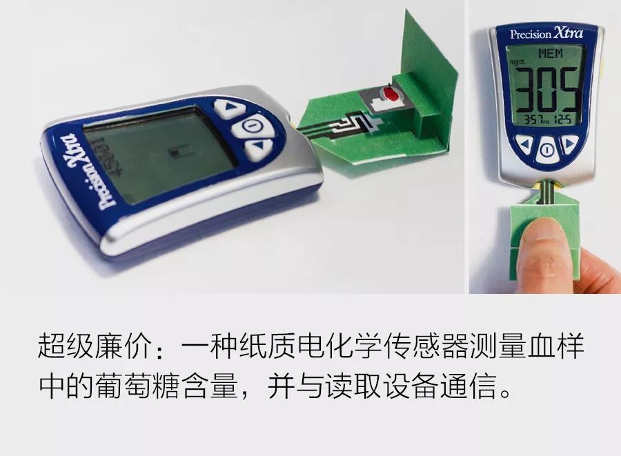
The research team of George Whitesides at Harvard University is exploring a method for a radio-frequency-readable paper-based medical diagnostic sensor. This paper sensor can provide visual readouts through color changes, just like home pregnancy test strips. By depositing wax and conductive inks using techniques such as screen printing and inkjet printing, Whitesides’ researchers have been able to manufacture paper-based microfluidic sensors, chemical sensors, humidity sensors, and even force sensors. Their goal is to create an affordable set of medical diagnostic sensors for developing countries. These devices can be bent, folded, and after use, can be burned with a match or allowed to decompose naturally. When we want billions of IoT sensors and products, their ability to decompose and return to nature can prevent landfills from being filled with obsolete Internet equipment.
Although many disposable sensors can utilize external radio frequency energy, some still require their own power source. This is why Allen’s team at the University of Pennsylvania is also exploring biodegradable electrochemical batteries made from the polymers and metals used to manufacture sensors. The saline environment in the human body provides the electrolyte for the battery, conveniently avoiding the toxic acids used in traditional batteries.
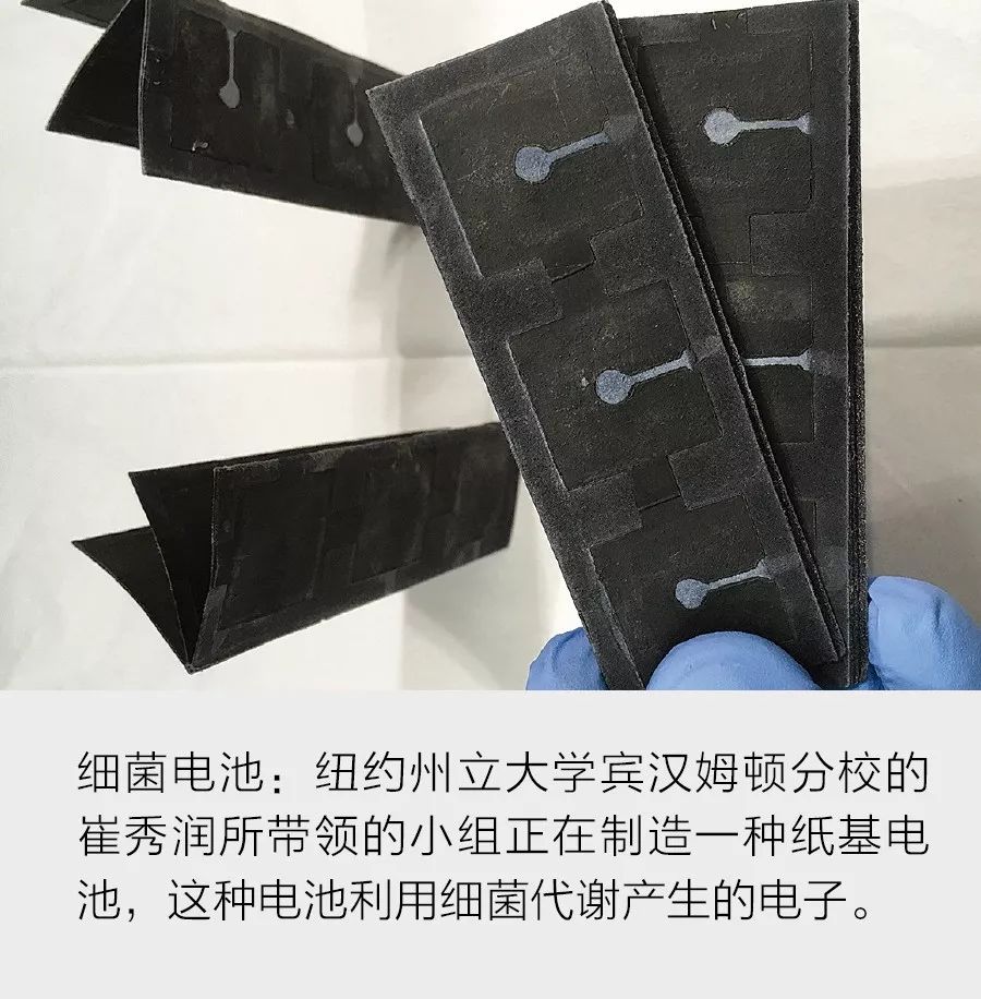
At Binghamton University, Seokheun Choi’s team is developing a paper-based battery that has a non-traditional electronic source—bacteria. Certain bacteria found in mud produce electrons while metabolizing food. These bacteria attach to metal electrodes printed on paper, and the metal electrodes collect the electrons emitted. Producing a few microamperes of current requires a stack of bacterial batteries, which can easily be achieved through origami—just fold the paper a few more times.
━━━━
Sensors typically require strict size control, and the flexibility of paper and plastic makes them difficult to use for manufacturing sensors. For instance, plastics can stretch and deform under slight changes in force or temperature. In the semiconductor industry, feature sizes have been controlled to within a few nanometers; the size of plastic parts can change by tens of microns due to just a few degrees of temperature increase. To achieve mass production of plastic and paper sensors, we need new, different design tools and manufacturing equipment.
However, paper processing and plastic processing technologies have been applied in other fields for decades, even centuries: paper printing presses and paper processing machinery used for producing newspapers and books; screen printing and inkjet nozzles used for precision printing; precision roll-to-roll plastic manufacturing used for producing magnetic tapes and edge tapes; and large-scale photolithography and thin-film deposition used for manufacturing rice-width liquid crystal television panels.
By repurposing these technologies to meet the specific needs of plastic and paper electronics manufacturing, a new emerging industry may soon be born. The U.S. Department of Defense has already begun to promote this new manufacturing infrastructure. In September 2016, the NextFlex center was inaugurated in San Jose, California. Organized by the U.S. Department of Defense, this project received $75 million in funding to promote the research and development of advanced manufacturing methods for flexible hybrid electronics. The goal of this center is to break away from the rigid framework of electronic products, namely printed circuit boards, which have relied on for the past 60 years for the design and manufacture of electronic systems.
Flexible hybrid electronics are the stepping stone to developing paper and plastic electronic products. They provide a practical compromise: we cannot yet manufacture high-performance transistors and other components on these substrates, but we can graft traditional silicon components, which are less than 50 microns thick (and thus become flexible), onto plastics, fabrics, and paper. The U.S. Department of Defense hopes that this manufacturing technology can provide lightweight and wearable electronic products for soldiers and military equipment in the short term.
In the long run, the development of new capabilities for manufacturing plastic and paper sensors and the accompanying business models will open up a new world of products. Compare this to the “fabless” model of chip manufacturing. When it emerged in the late 1980s, it quickly sparked a wave of large-scale design innovation. Young chip companies no longer bore the enormous capital expenditures of semiconductor fabs; they could focus on innovative designs while letting foundries handle the manufacturing work. The fabless manufacturing model accelerated the development of countless consumer electronic products, such as smartphones, tablets, and game consoles.
The manufacturing industry for plastic and paper electronic products may surpass the fabless model. Using simple materials and methods for production does not require facilities as complex as semiconductor fabs; every town or even every household may have a factory. This is a distributed manufacturing model. Today, we can already see 3D polymer printers in hobbyists’ home studios and professional machine shops. It is not hard to imagine that in 20 years, advanced 3D printers will also be able to manufacture flexible sensors and electronic products at home.
Of course, not all sensor technologies can be applied to plastics or papers. Many high-performance sensors (such as microphones and gyroscopes) still need to be made of silicon. This is because their physical performance depends on the properties of silicon, or on submicron tolerances that can only be achieved through traditional silicon micromachining. However, the simpler devices required for the massive consumer IoT, such as temperature, light, gas, or pressure sensors, will no longer use silicon but will use plastics or even paper. Consumer-oriented massive disposable IoT applications will only require sensors that are “good enough” in performance and low in price.
We are heading toward a watershed moment in electronic manufacturing between traditional silicon and emerging low-cost flexible substrates. New research advancements, the growing demand for flexible and low-cost sensors, and the increased awareness of reducing the environmental impact of electronic manufacturing will strongly drive plastic and paper sensor technology into the mainstream.
Source: Yuezhi Network. The original English text published in IEEE Spectrum can be viewed by clicking “Read Original”.

Click
Read Original
Learn more details