 Measurement and inspection technologies in semiconductor manufacturing are the “eyes” and “rulers” that ensure chip yield, performance, and reliability. The manufacturing of semiconductor wafers is akin to a marathon that spans 400 to 800 precise steps, each requiring meticulous attention and taking up to one to two months.
Therefore, at the critical nodes of the semiconductor manufacturing process, we must build a solid defense line for measurement and inspection. This is not only a barrier to protect product quality but also the cornerstone to ensure stable yield and smooth production. Through precise measurement and inspection, we can identify potential issues at the earliest opportunity, allowing for rapid strategy adjustments to ensure that the entire production process can proceed steadily and efficiently along the predetermined path.
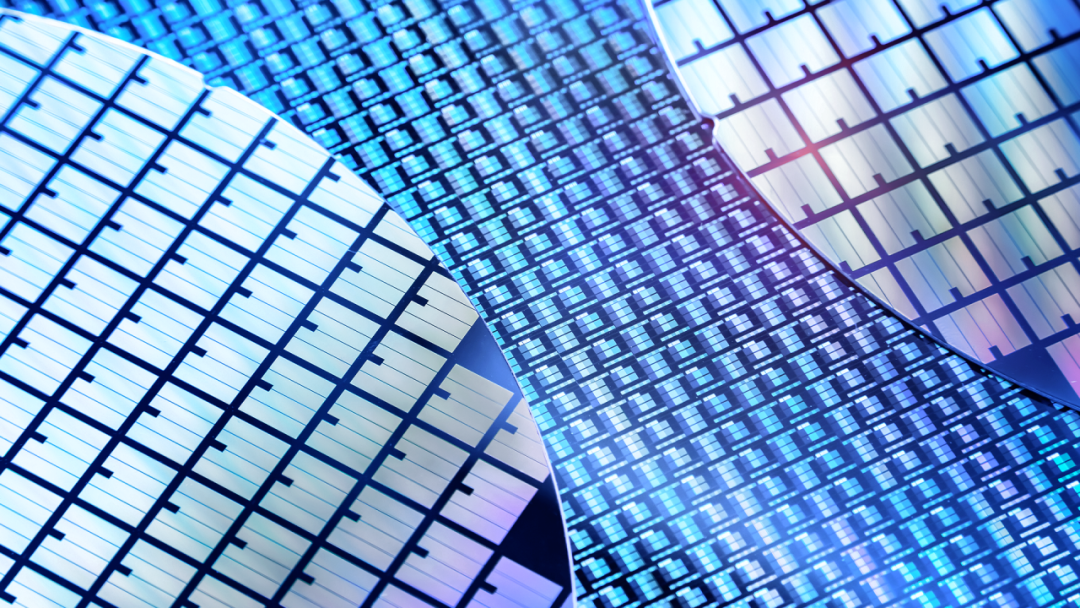 Measurement in Semiconductors
Measurement refers to the quantitative description of structural dimensions and material properties on the observed wafer circuits, such as film thickness, critical dimensions, etch depth, surface morphology, and other physical parameters.
01Ellipsometry and Spectral Reflectance Measurement
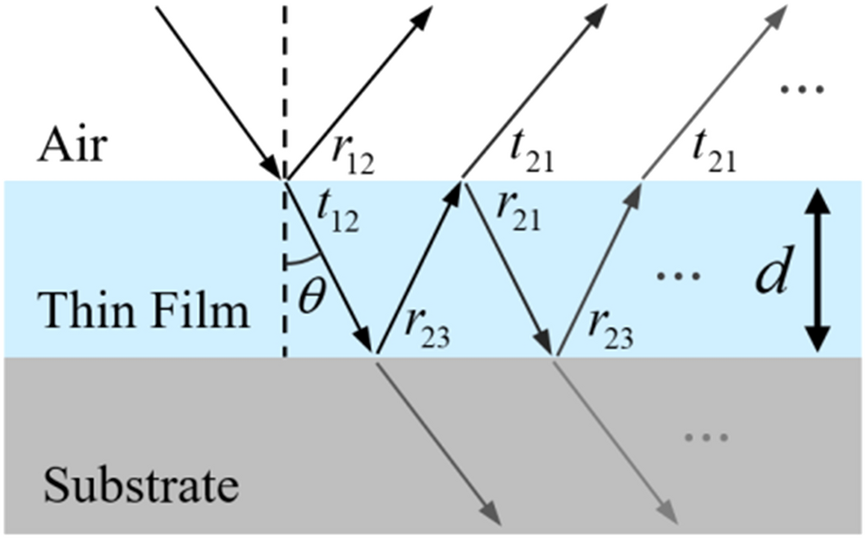
Ellipsometry and spectral reflectance measurement act like precise craftsmen, accurately calculating the thickness and optical properties of films by measuring the subtle changes of polarized light on the film and the reflected light spectrum on the film surface, ensuring the performance of semiconductors.
02Critical Dimension (CD) Measurement
In the field of critical dimension (CD) measurement, CD-SEM and Atomic Force Microscopy (AFM) serve as nano-scale rulers, measuring the critical dimensions of semiconductor devices and ensuring they precisely conform to design blueprints. Monitoring overlay errors is also a test of the close cooperation between each step of the process, ensuring that every note resonates harmoniously.
03Photomask and Mask Inspection
This is a strict control over pattern transfer. Optical inspection systems and EUV mask inspection act like precise inspectors, ensuring that every detail on the photomask is accurate.
04Electrical Characteristic Measurement
Electrical characteristic measurement acts like a magician revealing the intrinsic secrets of semiconductor materials. Four-point probe measurements and parameter analyzers reveal the true performance of semiconductor materials by measuring resistivity and electrical characteristic parameters.
05X-ray and X-ray Photoelectron Spectroscopy (XPS) Technology
X-ray and X-ray Photoelectron Spectroscopy (XPS) technology act like detectives in the chemical field, deeply analyzing the chemical composition, chemical bond states, and crystal structures of materials through X-ray photoelectron spectroscopy (XPS) and X-ray diffraction (XRD), providing a solid material foundation for semiconductor manufacturing.
06Chemical Mechanical Polishing (CMP) Measurement
In Chemical Mechanical Polishing (CMP) measurement, surface profilometers and thickness measurement instruments act like precise craftsmen, measuring the changes in surface flatness and film thickness after polishing, ensuring the semiconductor surface is flawless.
07Particle Detection and Surface Defect Detection
Particle detection and surface defect detection act like quality guardians, with particle counters and surface defect detection systems closely monitoring the particles and minute impurities on the wafer surface through optical and laser scanning methods, ensuring the purity of semiconductor products.
08Warp Measurement Technology
Warp measurement technology acts like a strict inspector, rigorously checking the curvature and warping of the wafer substrate and the stress of the film, ensuring the stability and reliability of semiconductor products in various environments.
Measurement Cases
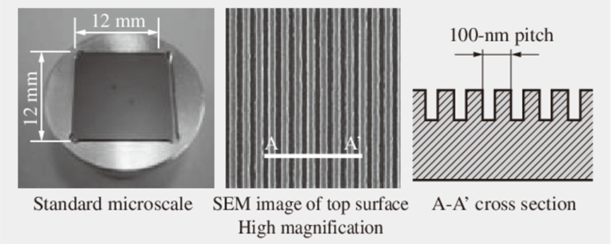
Measurement 1: Measuring the line width and aperture of circuit patterns at specified locations on the semiconductor wafer (CD-SEM).
Measurement 2: Measuring the thickness of the surface film on the semiconductor chip (ellipsometer, etc.)
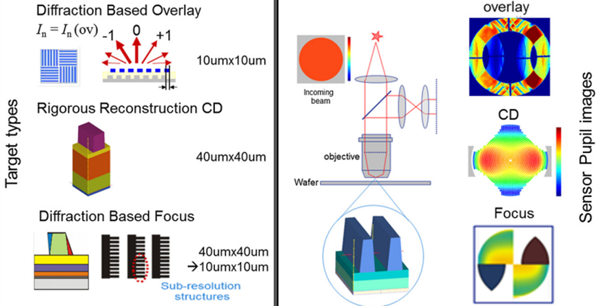
Measurement 3: Measurement system used to detect overlay accuracy (stepper). Performing measurements to detect the accuracy of the overlap between the first and second layer patterns transferred to the wafer.
 Inspection in Semiconductors
In the precise world of semiconductor manufacturing, inspection equipment acts like a strict proctor, meticulously examining every speck of dust and every flaw in the wafer according to established standards. This process, aims to accurately capture the hidden locations of defects, namely their coordinates (X, Y), ensuring that every detail meets perfect standards.
However, the sources of these defects are often elusive; they may be dust floating in the air or particles inadvertently adhered. Once the wafer surface is occupied by these uninvited guests, the drawing of circuit patterns will be disrupted, leading to missing patterns, which in turn hinders the normal operation of electronic circuits, rendering the wafer a defective product.
Therefore, defect detection and process monitoring are particularly critical in semiconductor manufacturing. They act like guardians, constantly overseeing every step of the manufacturing process to ensure that perfect devices that meet design requirements can ultimately be produced.
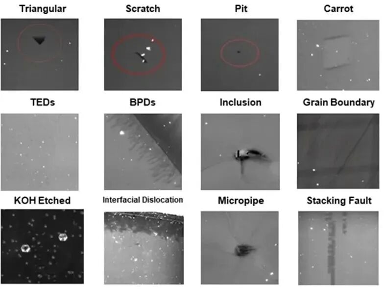 01Optical Inspection Technology
Optical inspection technology is a commonly used defect detection method in semiconductor manufacturing. It has the advantages of speed and relatively low cost.
However, due to the limitations of optical diffraction, optical inspection technology may encounter difficulties in detecting nano-scale defects.
Nevertheless, optical inspection can still be used for early-stage defect detection, helping to quickly identify potential problem areas for subsequent detailed analysis.
Automated Optical Inspection (AOI) equipment is often used to detect surface defects on printed circuit boards (PCBs) by scanning and detecting potential defects.
02Scanning Electron Microscope (SEM)
The Scanning Electron Microscope (SEM) is a technique that uses an electron beam to scan the surface of a sample to generate high-resolution images. SEM plays a key role in semiconductor defect analysis, capable of detecting and analyzing nano-scale defects. The main advantage of SEM lies in its high-resolution imaging capability, which can clearly display the morphology and size of defects. Some important applications of SEM include:
Defect Detection and Classification: SEM can be used to detect various types of defects, such as particles, scratches, cracks, and film defects. By analyzing SEM images, defects can be classified into different types, helping to determine the root cause of the defects.
Defect Review: SEM is often used as a defect review tool to verify and analyze defects found by other detection technologies (such as optical inspection).
Automated Defect Detection: By combining machine learning and deep learning algorithms, automated defect detection and classification of SEM images can be achieved, improving detection efficiency and accuracy.
To enhance the detection capabilities of SEM, researchers are continuously developing new algorithms and techniques. For example, a dual-branch CNN-Transformer architecture (DeepSEM-Net) has been proposed to enhance defect classification and precise segmentation in SEM defect analysis. Additionally, a deep learning framework based on Faster R-CNN has been developed to identify and classify defects in SEM images.
03Transmission Electron Microscope (TEM)
The Transmission Electron Microscope (TEM) is a technique that uses an electron beam to penetrate a sample to generate images. TEM has a higher resolution than SEM, allowing observation of the atomic structure of materials. TEM is mainly used in semiconductor defect analysis for:
High-Resolution Imaging: TEM can provide atomic-level images of materials, allowing analysis of lattice structures, interfaces, and microscopic details of defects.
Material Analysis: TEM can be combined with techniques such as Energy Dispersive X-ray Spectroscopy (EDX) to analyze the chemical composition and elemental distribution of defects.
3D Reconstruction: By tilting the sample and acquiring a series of TEM images, 3D reconstruction can be performed to understand the three-dimensional morphology of defects.
04Other Advanced Analysis Methods
In addition to optical inspection, SEM, and TEM, many other advanced analysis methods are used for semiconductor defect analysis, including:
Atomic Force Microscopy (AFM): AFM can measure the surface morphology and mechanical properties of materials with nanometer resolution. AFM can be used to detect and analyze surface defects, film thickness, and roughness.
Secondary Ion Mass Spectrometry (SIMS): SIMS is a technique used to analyze the surface composition of materials. SIMS can be used to detect and quantify impurities and dopants in materials, helping to determine the source of defects.
Laser Ultrasonic Technology: By using laser ultrasonic technology, imaging characteristics of different defects in metallic materials, such as pores and cracks, can be obtained, allowing for the assessment of the performance of metal components.
Time-Frequency Domain Acoustic and Thermal Signal Analysis: By combining machine learning, the robustness and accuracy of non-destructive fault identification can be enhanced. Experiments using Scanning Acoustic Microscopy (SAM) are conducted, and time-domain signals are converted to frequency-domain signals using Fast Fourier Transform (FFT), followed by classification and defect detection using machine learning.
END
Source | Semiconductor Science in Ten Minutes, YouShuo. Images sourced from the internet, copyright belongs to the original author. If there are any infringement issues, please contact us for removal. Thank you very much.
Previous RecommendationsRECOMMEND1
Breaking! IF13.3, Top Journal in Area 1 of the Chinese Academy of Sciences Removed!
2Understand GC-MS in 3 Minutes: From Drug Testing to Food Safety, Why is This Instrument Ubiquitous?3Graduate Students Still Engaged in Research During Summer Vacation? It Seems Crazy, But They Have No Choice…PS: Kexing Testing can provide in-situ scanning servicesThose in need can scan the QR code below for detailsThe specific in-situ scanning prices are as follows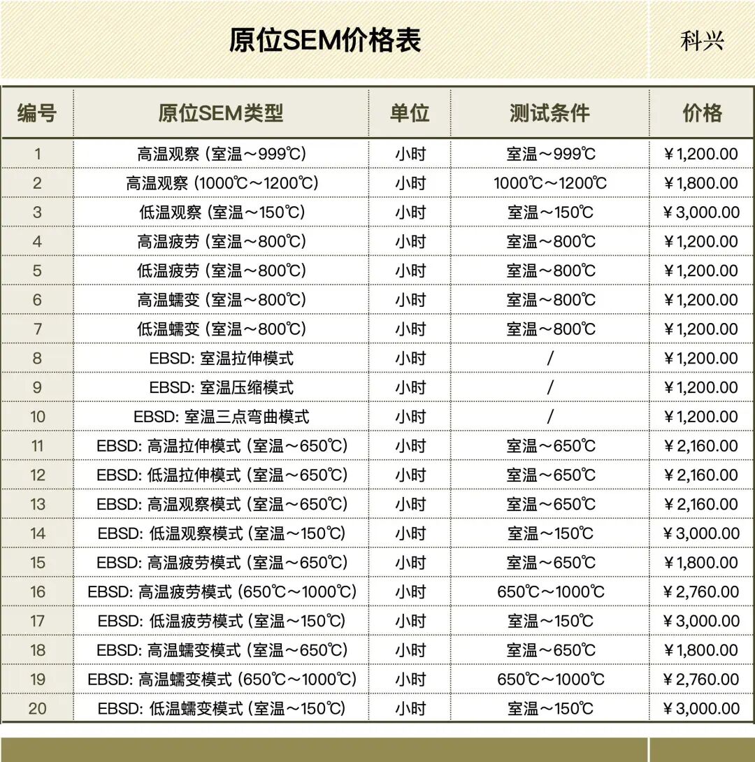 Welcome customers and friends to make sampling appointments!